

Research Article - (2022) Volume 6, Issue 2
Modeling Arc less Ingap/Gaas Double Junction Solar Cell with Tunneling Junction and Bsf Layer
2Department of Electrical Engineering, Damavand Branch, Islamic Azad University, Tehran, Iran
3Electrical Engineering Department, Tabriz Branch, Islamic Azad University, Tabriz, Iran
Received Date: Sep 02, 2022 / Accepted Date: Sep 09, 2022 / Published Date: Oct 12, 2022
Copyright: ©Copyright: ©2022 Nemat azimi. This is an open-access article distributed under the terms of the Creative Commons Attribution License, which permits unrestricted use, distribution, and reproduction in any medium, provided the original author and source are credited.
Citation: Azimi, N., Ghari, S., Saghai, H.R. (2022). Modeling ARC less InGaP/GaAs Double Junction Solar cell with Tunneling Junction and BSF layer. Stem Cell Res Int, 6(2), 100-109.
Abstract
The present study addresses the structure of InGaP/GaAs dual-junction (DJ) solar cells by introducing new buffer and back surface field (BSF) layers as well as selecting the appropriate material for the tunnel junction. Different performance parameters including open-circuit voltage (�??oc) short-circuit current density (ð½ï¿½??ð¶), fill factor (ð¹ð¹), and solar cell efficiency (�??) were proposed and extracted for comparison with literature results. Then, I-V characteristic curves for the model were represented in graphs. The mentioned parameters, i.e. open-circuit voltage �??�??ð¶, short-circuit current density ð½ï¿½??ð¶, fill factor ð¹ð¹, and solar cell efficiency �?? were, respectively, obtained as 18.50 �??ð´/�?��??2, 2.862 V, 87/32 percent and 46.23 percent (1sun) under AM1.5G spectrum, which indicates the improvement achieved in this study.
Keywords
Dual-junction (DJ), Solar Cell, Tunnel Junction, Back Surface Field (BSF)
Introduction
In multi- junction (mj) solar cell, communication between each of the sub-cells is possible through a tunnel junction. The tunnel junction should have low resistance to minimize voltage drop be- tween cells and should also have high light transmission capability to minimize current loss due to light absorption within the tunnel junction layers. In this layer electrons tunnel between the potential barriers formed at the surface of the bilayer interface. Electrons cross a narrow, constant-energy barrier when energies with a poten- tial greater than the barrier. The main purpose of tunnel junctions is to create low electrical resistance and loss between two sub-cells [1].Without a tunnel junction, the p-impurity region in the upper cell communicates with the n-impurity region in the middle cell, in which case a p-n bond is formed in the opposite direction between the upper and middle cells. As a result, multi-bonded solar cells between the n-p layers need an interface to prevent parasitic bond- ing. Due to the placement of the layers on top of each other, tun- neling junction is used to prevent the formation of parasitic bonds. The tunnel junction consists of a high-dose doped p-n bond placed between the n-p bilayers as a transition layer. However, it should be noted that the structure with tunnel junction in direct bias has a smaller voltage drop than the cell structure without tunnel junction [2]. In this paper, tunnel junction, which is effective as a key pa- rameter in increasing the efficiency of solar cells, is evaluated and the most optimal tunnel junction structure using quantum tunnel- ing model based on trap connections and band to tunnel non-local band by The Wentzel-Kramers-Brillouin method is defined, and based on this, a complete modeling of the gallium arsenide-based solar cell structure is performed. In this simulation, anti-reflective coating is used to increase the efficiency.
Also, a sample of a three-link solar cell with a tunnel junction structure has been optimized and a yield of 34.15% has been re- ported [3]. In this study, two important materials AlGaAs and In- AlGaP with different thicknesses for high and low BSF cells were investigated using Silvaco ATLAS numerical calculation modeling tool. It has also been shown that under the conditions of matching the current with the thinner upper BSF layer and the thicker low- er BSF layer, the Jsc short-circuit current density and the Voc in- crease, thus improving the overall efficiency of the solar cell. Also, the efficiency is equal to 32.196%, which in comparison with other cells studied in this study, shows an increase in efficiency in solar radiation [4]. In another paper, calculations have been performed for multinucleated cells consisting of upper AlGaAs cell, middle GaAs cell and lower InGaAs cell in order to achieve the optimal band gap and thickness for each bond under AM1.5 solar radiation.
To reduce natural reflection, an anti-reflective coating is placed on the device to significantly increase the current density com- pared to the previous state. Finally, according to the simulations performed, it was found that the conversion efficiency of this cell has increased to about 28.5%. Light improves the efficiency is op- timized by changing the thickness of the upper BSF layer. From the result it is quite clear that the high cell photon absorption is suitable for wavelengths less than 610 nm, while the lower cell absorption is suitable for wavelengths between 900-500 nm. Also, the optimized BSF material (P0.5 (Ga0.3 Al0.7)0.5 in is compat- ible with InGaP and GaAs. Finally, due to the changes made, the conversion efficiency of the device is 39.1% (1000 sun) and 34.52 in another article, a solar cell with an InGaP / GaAs tunnel junction is proposed, which is designed to provide more transparency for the lower cell as well as to reduce the recombination effects.
Optimized to achieve higher gain, the simulations were performed in 1000 sun radiation of AM1.5G spectrum, and according to the performed simulations, the efficiency value was estimated to be 40.603% [7]. The BSF layer plays a very prominent role for single- junction and multi- junction (MJ) solar cell to control the recom- bination rate. In the last study, the performance of a Dual-junction solar cell InGaP/GaAs is modified by the addition of a thin layer of carbon nanotubes (CNTs). Carbon nanotubes (CNTs) have a wide range of direct band gaps matching the solar spectrum and strong absorption of infrared and ultraviolet light, which makes them an ideal photovoltaic material. Finally, the efficiency of this cell is 40.95% [9].
Performance Parameters of Solar Cells
Solar cells based on the photovoltaic effect are used to convert the sun's light power into electricity [10]. When the p-n bond is exposed to sunlight, pairs of electrons and holes are produced by photons whose energy is greater than the band gap. The number of electron-hole pairs produced is proportional to the amount of light emitted. When the p-n junction is exposed to sunlight and in open circuit, voltage is generated due to the separation of the charge carriers.
When the p and n sides are short-circuited, the current generated is called the short-circuit current Isc and is equal to the generated optical current IL (if the series resistors are zero). When the p and n sides are separated, the electrons move to n and the holes move to p, resulting in an electric potential. The voltage provided is called the open circuit voltage Voc.
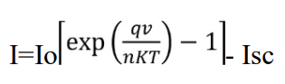
The current-voltage characteristic of the p-n junction in the case of light radiation is as follows:
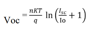
The open circuit voltage is obtained by considering I = 0:
When the solar cell is operating at maximum output power, it will be at the optimum operating point of voltage Vm and current Im [11].
The values of Isc and Voc depend on the type of semiconductor. We see lower energy gap semiconductors, such as germanium, lower Voc, and higher Isc, while larger energy gap semiconduc- tors, such as InGaP, have inverse characteristics. The solar cell is modeled as a current source parallel to a diode. When light shines on the cell surface, a stream of light is produced;
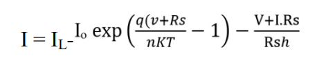
Where Rs and Rsh represent the series and parallel resistors and IL of the photovoltaic current produced. In the equivalent circuit of the solar cell, the resistors Rs and Rp are used as series and parallel resistors of the solar cell, and Iph is used as the generated electric current of light in the cell exposed to light. The power delivered by the solar cell is the product of current and voltage. If the point multiplication operation is performed for all open circuit voltages and short circuit currents.
Although the short-circuit current at the zero point is maximum, the voltage and power are zero. The voltage and current state at the open circuit point is inverse, and again at this point the power is zero. There is a special combination of current and voltage that leads to maximum power. This is the maximum power point. The point (Max P) actually represents the operating point at which the solar cell can provide the maximum power for a given intensity of radiation. The corresponding values of Vmp and Imp can be estimated from Voc and Isc as follows:
If Imp and Vmp represent the current and voltage of the cell at maximum power, respectively, the maximum power of the cell is expressed as follows [12]:
Pmax= Imp Vmp = VocIscFF
Where FF is defined as the cell filling coefficient. The charge fac- tor (FF) is actually a measure of the quality of solar cells. A higher charge factor for a solar cell means that the solar cell has a better efficiency for converting solar energy into electricity. This coeffi- cient is often shown as a percentage [13].

The solar cell power conversion efficiency η is defined as the ratio of the maximum electrical power generated by the output to the to- tal power of the Pin radiated light. In order to improve efficiency, it is necessary to maximize all three parameters Voc, Isc and FF [11].
Presenting New Structure, Simulation and Analysis 1-3 Expo- sure with Am1.5g
Numerical simulation of this design obtained under AM1.5G (1sun) radiation. The numerical diagram of this spectrum created using the simulation in Silvaco ATLAS program is very similar to the AM1.5G spectrum.
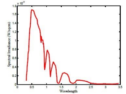
Figure 1: AM1.5G solar spectrum
A high InGaP cell with a band gap of 1.8 electron volts is used to absorb photons in the ultraviolet and visible spectrum. Whereas, the low GaAs cell with a band gap of 1.42 electron volts is used for energetic photons with a near-infrared band gap. InGaP, GaAs, and InAlGaP are very effective in absorbing photons that have energy close to their band gap energy.
Tunneling Behavior
A tunnel junction with heavy contamination and small thickness electrically and optically connects the upper InGaP cell and the lower GaAs cell. This region leads to recombination between elec- trons and holes in the top and bottom cells, respectively. Figure 2 shows a diagram of dual- junction InGaP/GaAs solar cell powers / powered strip made with Silvaco ATLAS software at zero volts after adjusting the material parameters.
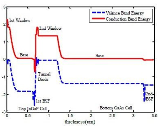
Figure 2: The curves valence and conduction bands Ingap / Gaas dual-Junction (Dj) solar cell
The tunneling area is approximately 0.695 μm. As can be seen from the results, the InAlGaP window layer with larger band gap energy (2.36 electron volts) is used for optimum transparency and emitter coating. Reduce the effects of surface recombination.
Adding a Buffer Layer to the Bottom Cell and Optimizing the Dual-Junction (Dj) Solar Cell Ingap / Gaas
To achieve greater efficiency, an additional layer called a buffer layer is added to the bottom cell, which is necessary to achieve maximum efficiency. According to Table 1, it can be seen that the properties of the materials used in this design are similar and make them quite desirable materials. The current device structure con- sists of a buffer layer next to the cathode electrode. The main role of the buffer is to collect and transfer load carriers and prevent opposing loads. The use of a cathode buffer layer also makes it possible to build highly efficient solar cells. It is expected that the photovoltaic parameters will be mainly affected by the electrode buffer layer, which is usually Voc, maximized at ohmic junctions, and the FF fill factor coefficient is also improved. The proposed hardware structure, along with the exact contamination profile and thickness, is shown in Figure 3.
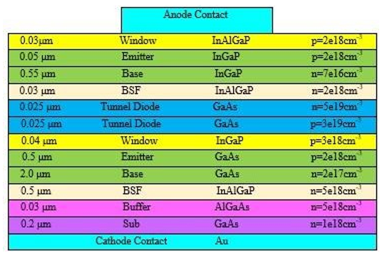
Figure 3: Schematic diagram of the Dual-junction (DJ) solar cell InGaP / GaAs
In this design, the buffer layer is used to achieve greater efficien- cy. The buffer layer provides a conductive strip that improves the performance of the device (Figure 4a). The spikepart prevents Voc open circuit voltage losses due to the recombination level control. The created barrier prevents the transfer of less energetic electrons and therefore causes a low level of recombination in this layer. As you can see in Figure 4, it has higher alpha and more band gap than InAlGaP, and for this reason, the optical production rate of this layer is also higher than AlGaAs and the light flux increases slightly after adding the buffer layer. (Figure 4 b)
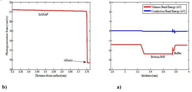
Figure 4 a): The curves valence and conduction bands of BSF layer and bottom cell buffer
b) Comparison of optical production rate of BSF dual layer bottom cell.
AlGaAs buffer layer can be effective in increasing Voc and Jsc. The combination of AlGaAs with other layers leads to an increase in lower light current due to the increased recombination in the emitter layer of the bottom cell, but the rate of light production is also high. Solar cell performance is possible by changing the thickness of the AlGaAs buffer layer to optimize and achieve max- imum efficiency. Important simulation parameters are possible to optimize and achieve maximum efficiency. The important param- eters of the proposed solar cell simulation are shown in Table 1.
Table 1: Effect of AlGa As buffer layer thickness change on the proposed solar cell profile
|
Eff (%) |
FF(%) |
Voc(V) |
Jsc(mA/cm2) |
Thickness (μm) |
|
36.4212 |
87.1287 |
2.2300 |
16.3278 |
0.01 |
|
36.5742 |
87.9267 |
2.2310 |
16.3936 |
0.02 |
|
36.7806 |
87.9341 |
2.2320 |
16.4846 |
0.03 |
|
36.7910 |
87.9201 |
2.2320 |
16.4893 |
0.04 |
|
36.7885 |
87.9138 |
2.2318 |
16.4755 |
0.05 |
In the previous case, it has increased by about 0.573 %, which can be increased after the next changes. The table of efficiency chang- es based on the thickness of the buffer layer is shown in Table 1. According to the diagram, it is clear that at a thickness of 0.04 micrometers, the efficiency of the device reaches its maximum.
The effect of changing the type of tunnel junction material on the solar cell characteristics of Dual junction InGaP / GaAs grafts In this section, we examine the change in tunnel junction materi- als on the structure of Dual-junction (DJ) solar cell. As mentioned earlier, in multi- junction (MJ) solar cell, communication between each cell is possible through a tunnel junction. Tunnel joints should be transparent to the wavelength absorbed by the next photovoltaic cell. Here, the tunnel junction consists of a high-dose contaminat- ed p-n bond with low resistance to minimize voltage drop between cells. It also has high optical transmission capability to reduce light loss due to light absorption within the tunnel junction layers. At this junction, electrons tunnel between the potential barriers formed at the interface of the bilayer.
In this design, the main purpose of the tunnel junction is to create low electrical resistance and little loss between the two cells. With- out a tunnel junction, the impurity region p interacts with the im- purity region of upper and lower cells, in the middle of two cells, and a p-n bond is formed in the opposite direction of the top upper and bottom cells. As a result, the multi-bonded solar cell between the p-n layers needs an interface. Tunnel junction increases the efficiency of several bond solar cells by creating a low resistance pathway for carriers to flow. Table 2 shows the performance of a Dualjunction solar cell with a tunnel area composed of different compounds.
Table 2: Proposed different solar cell parameters with different materials in the tunnel junction area
|
Eff(%) |
FF(%) |
Voc(V) |
Jsc(mA/cm2) |
Material |
|
36.7806 |
87.9341 |
2.2320 |
16.4787 |
GaAs/GaAs |
|
36.6242 |
87.9267 |
2.2321 |
16.4079 |
AlGaAs/GaAs |
|
36.6076 |
87.9341 |
2.2321 |
16.4005 |
InGaP/GaAs |
|
36.8608 |
87.9201 |
2.2340 |
16.4999 |
InGaP/InGaP |
Here, InGaP is used as an alternative. The proposed solar cell struc- ture consists of three regions: top cell, tunnel diode, and Bottom cell. The schematic of the proposed structure is shown in Figure 5.

Figure 5: Schematic structure of InGaP / GaAs Dual junction solar cells layer after replacement of InGaP
Material with Gaas in the Tunnel Junction Area We know that one of the most important issues for achieving high efficiency of integrated multi- junction solar cell is to achieve low- loss electrical and optical connections. InGaP is a very popular substance in solar cells. InGaP is a large bandwidth semiconductor with network compatibility with GaAs. Also, the band gap of this material is bigger compared to GaAs. The materials of the differ- ent layers of the solar cell are selected so that the band gap of the upper layers is the largest and then the solar cell is continued by tunnel junction and the band gap will be less in the bottom layer Eg (top cell) > Eg (tunnel diode) > Eg (bottom cell) Since it is difficult to achieve the maximum tunneling current in the upper band gap, it is necessary to form a thin discharge zone with high pollution. Most potential drops occur throughout the p-n graft discharge re- gion. Figure 6 this is due to the presence of endogenous potential during n-p bond formation.
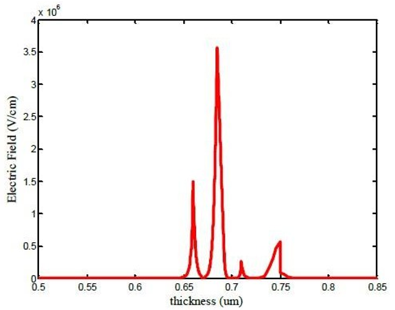
Figure 6: Electric field in the tunnel junction area
The voltage drop across the junction is due to the built-in potential, so that the electric field in the junction region is maximam. Figure 7 shows the electric field developed in the various layers of the modeled solar cell. The field in the junction area is clearly very large.
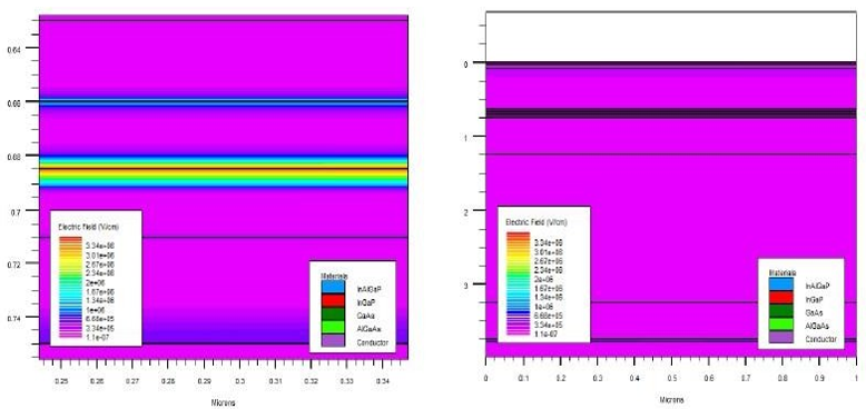
Figure 7: b) Electric field in tunnel junction A): Electric field of different layers
According to the above criteria, efficient absorption of solar ra- diation by different layers of the solar cell results in higher effi- ciency. By replacing InGaP with GaAs, the efficiency increases to 36.8608%. This proves that the InGaP/InGaP tunnel junction performs better than the GaAs/GaAs tunnel junction.
Adding a Bsf Layer to the Top Cell and Optimizing In the previous section, it was said that an effective BSF layer is an important element in achieving a high efficiency of a solar cell. This layer, which we are considering in this section, is an import- ant layer in the structure of the solar cell that prevents the charge carriers from recombining by returning them to the p-n junction. These layers are applied to consecutive or junction III-V solar cells. A key feature of the BSF layer is that it limits participation for optically produced carriers and maintains them in p-n junction expansion without increasing the series resistance of the device. This layer also acts as a reflector of minority carriers to the p-n junction.
Optimizing the thickness of the BSF layer is a very important point in the design of multi- junction (MJ) solar cell. By changing the thickness of this layer, large changes can be made in the open cir- cuit voltage and Short-circuit current of the device. In this work, InAlGaP material is used as the BSF layer, which is network com- patible with GaAs material. The presence of BSF multilayers leads to more aggregation of optically produced carriers. It also creates a very strong potential barrier to prevent minority carriers and re- combination between layers.
According to the above description, in addition to the existing 30 nm thick InAlGaP BSF layer, another BSF layer (according to the research) [2] has been introduced on top of the existing BSF with a lower contamination concentration. The proposed hardware struc- ture consists of a high BSF bilayer with an exact contamination profile and thickness shown in Figure 8.
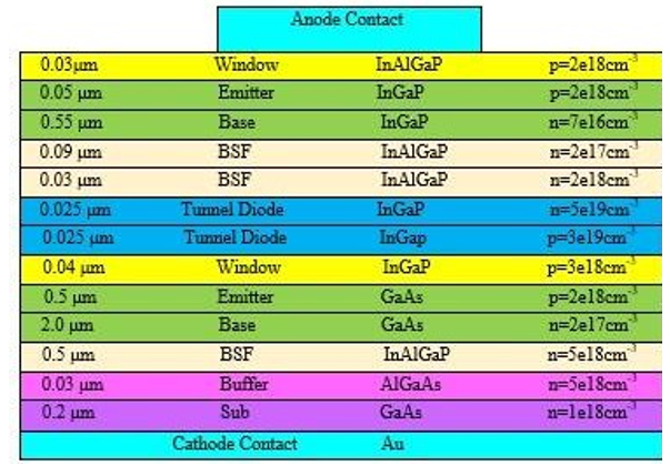
Figure 8: Proposed Dual-junction (DJ) Solar Cell proposed InGaP/ GaAs bonds with BSF bilayers above
In order to improve the performance of the solar cell, modeling and complete optimization of the various layers of the device is essential. Upper cell optimization is performed by keeping all bot- tom cell parameters constant. The lower thickness of the upper cell is a very important point in the design of Dual-junction solar cells. Because less thickness makes the bottom cell more transparent. Due to the characteristics of the BSF layer, more than one BSF layer has been used in this design.
Most solar cells have a recombination problem. Just when the load carriers are away from the field, recombination occurs when the carriers are shrinking, which directly reduces the efficiency. The BSF layer not only prevents the recombination of carriers, but it is necessary to consider it to increase the overall efficiency of the device. To overcome this problem, we placed another layer of BSF in the top cell to absorb the reflected minority carriers and the ma- jority carriers.
The absorption coefficient of the material is a limited value. There- fore, for a finite layer, it is not possible to absorb all the landing light If the energy of the landed photon is close to the band gap of the material and the absorption coefficient is smaller than the band gap, light will pass through the material. Thus, the thinner the cell, the more it transmits photons. For a double-bonded cell, the thinning of a layer from the top cell helps distribute light to the lower cell to increase the flow of the top cell. As a result, the top cell should be as thin as possible to allow for higher yields. The generated potential in all layers is shown in Figure 9.
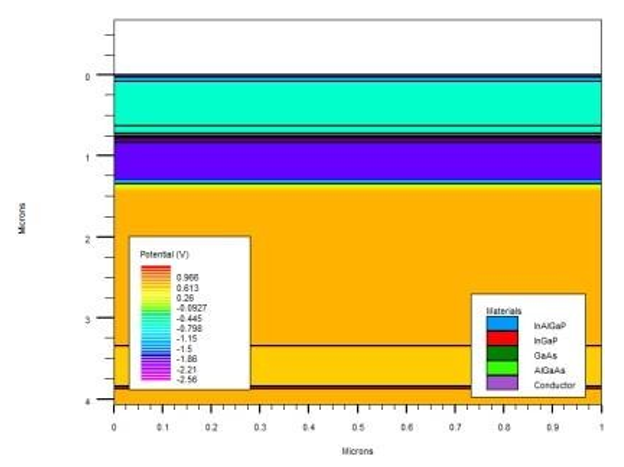
Figure 9: Potential of the proposed structure
Most of the current produced in the solar cell is mainly produced in the upper cell. Because the upper cell absorbs all the higher energy photons and creates a large number of electron pairs in the cavity. The greatest potential produced is in the area of the tunnel junction. As can be seen, the potential decrease in areas far from the tunnel junction.
We know that the photo generation rate nothing more than measur- ing the number of carriers produced in each layer of the cell in the presence of radiation. High optical production rate leads to higher efficiency. As the cell operates over a wider range of wavelengths, this rate depends on the optical properties of the material. As we move away from the surface, the photo generation rate gradually decreases. In the BSF layer, the dispersion of carriers is very low. Therefore, in the BSF region, the photo generation rate is very high, which can be clearly seen in Figure 11. The upper solar cell is also optimized by keeping all the lower cell parameters constant. Figures 10 and 11 shows the rate of photo generation rate in the solar cell during radiation.

Figure 10: photo generation rates in the model

Figure 11: Details of the photo generation rate in different layers
To analyze the effect of the BSF layer, to achieve the best efficien- cy, we changed the thickness of this layer in the upper cell. The results of the changes are listed in Table 3. It is quite clear from Table 3 that at a thickness of 90 nm, the amount of efficiency will be maximized.
Table 3: Different parameters of the solar cell by changing the thickness of the new BSF layer
|
Eff(%) |
FF(%) |
Voc(V) |
Jsc(mA/cm2) |
Thickness (μm) |
|
38.8212 |
88.4602 |
2.8563 |
15.3644 |
0.01 |
|
40.5742 |
88.2485 |
2.8579 |
16.0877 |
0.03 |
|
42.7806 |
88.1041 |
2.8582 |
16.4846 |
0.05 |
|
45.8910 |
87.9201 |
2.8591 |
16.9886 |
0.07 |
|
46.2356 |
87.3216 |
2.8620 |
18.5012 |
0.09 |
|
46.0163 |
87.4206 |
2.8510 |
18.4282 |
0.1 |
Comparison of Important Indicators of the Presented Structure
In this section, we compare the most important structural features presented in this chapter. The voltage characteristics of the prima- ry solar cell and the proposed solar cell are presented in the previ- ous section and their specifications are also obtained in the related sections. We have also compared the results obtained in this sec- tion. From the initial results, it was observed that the performance and results of the simulated multi- junction (MJ) model are very similar to the research [4]. According to the study [4], the results are comparable to the experimental data of the produced cells. The desired results are compared with experimental data related to similar devices using the same parameters. Their only differences are due to changes in the materials and optical parameters used. The curves obtained from the structure show very similar results to the experimental values.
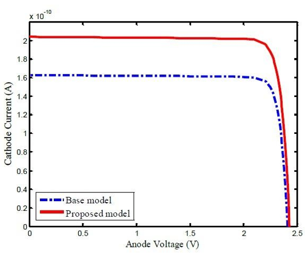
Figure 12: Characteristic curve I-V of the primary solar cell (blue dot line curve) and solar cell Proposed (continuous red line curve)
After the completion of the optimizations and simulations of the proposed structure, the values of Jsc, Voc, FF and Eff were ob- tained as 18.50 mA/ cm2 , 2.42 volts, 87.32% and 46.23%, respec- tively. The I-V characteristics produced in the initial design and the final design proposed in this research can be seen in Figure 12.
Table 4: Comparison of important parameters of the proposed design and other designs
|
Solar Cell |
Voc(V) |
Jsc(mA/cm2) |
Sun |
FF(%) |
Eff(%) |
|
[14] |
2.320 |
10.9 |
1 |
79.00 |
23.600 |
|
[15] |
2.300 |
10.6 |
1 |
87.55 |
25.140 |
|
[4] |
2.390 |
16.1 |
1 |
87.52 |
32.196 |
|
[6] |
2.660 |
17.33 |
1 |
88.67 |
39.150 |
|
[16] |
2.668 |
18.23 |
1 |
88.29 |
40.879 |
|
[17] |
1.04 |
33.23 |
1 |
86.43 |
29.18 |
|
[18] |
3.13 |
19.99 |
1 |
88.12 |
38.79 |
|
Proposed model |
2.42 |
18.50 |
1 |
87.32 |
46.23 |
As can be seen, the final model has higher Voc and Jsc, which help to increase the efficiency of the device. A comparison of the important parameters of the proposed design with other related de- signs is shown in Table 4. According to the values in this table, Eff and JSC show a significant increase. Also in the proposed model, the photo generation rate in the upper BSF layer is high. Therefore, the density of the generated current will increase and the efficiency of the cell will improve compared to the original design.
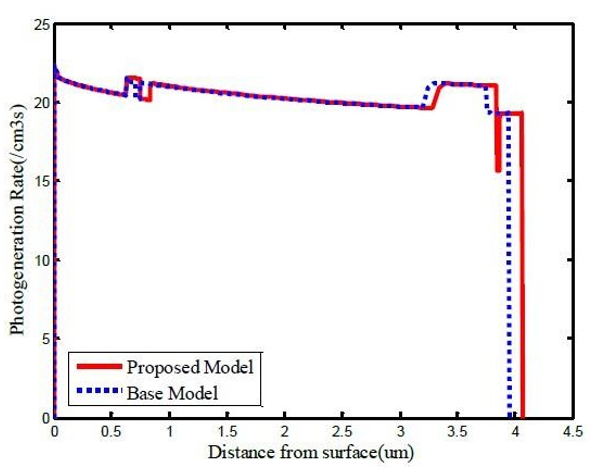
Figure 13: Comparison chart of photo generation rate of primary solar cell and proposed solar cell; Optical production rate of the original design (blue line (; proposed optical production rate) con- tinuous red line)
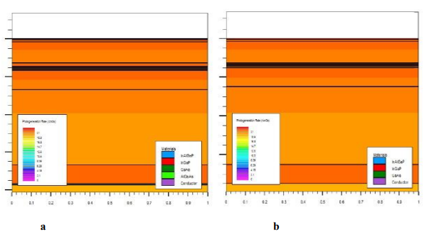
Figure 14: Comparison of photo generation rate of solar cells; A)Optical production of primary solar cell;
B) Optical production of proposed solar cell
Conclusion
In this paper, optical simulation Dual-junction Solar Cell of InGaP / GaAs is presented. With careful modeling, the prototype was sim- ulated to show the correct operation of the solar cell. Silvaco Atlas program was used to provide simulation and analysis of the de- vice. Then, the structure Dual-junction Solar Cell of InGaP/GaAs was modified, step by step, optimized, and optimized to achieve the desired performance. Solar cell performance was evaluated by adding BSF layer to the cell and changing the layer thickness. The simulation results showed that by doing this, the energy absorption is increase and the photo generation rate is increased, and as a result, the current of the device is higher, which will increase the efficiency of the cell.
The new structure significantly increases cell efficiency compared to the original structure, as well as the proposed solar cell flow. But according to Voc, the designed solar cell has a voltage almost equal to the original design. After completing the simulation of this step, the efficiency of the device increased to 46.23%. sum- marizing the results of this project, it can be concluded that the Dual-junction Solar Cell of InGaP / GaAs by optimizing the BSF layer with InGaP / InGaP tunnel junction and the buffer layer, the solar cell performance according to Voc, Jsc conditions. And the efficiency has increased dramatically, and considering the optimi- zation of the BSF layers and the introduction of the optimal tunnel junction, it has an extremely better efficiency.
References
- Al-Naser, Q. A. H., Hilou, H. W., & Abdulkader, A. F. (2009, August). The last development in III-V multi-junction solar cells. In 2009 ISECS International Colloquium on Comput- ing, Communication, Control, and Management (Vol. 1, pp. 373-378). IEEE.
- Dutta, J. P., Nayak, P. P., & Mishra, G. P. (2016). Design and evaluation of ARC less InGaP/GaAs DJ solar cell with InGaP tunnel junction and optimized double top BSF layer. Optik, 127(8), 4156-4161.
- Babar, M., Rizvi, A. A., Al-Ammar, E. A., & Malik, N. H. (2014). Analytical model of multi-junction solar cell. Arabian Journal for Science and Engineering, 39(1), 547-555.
- Singh, K. J., & Sarkar, S. K. (2015). Highly efficient ARC less InGaP/GaAs DJ solar cell numerical modeling using op- timized InAlGaP BSF layers. Optical and Quantum Electron- ics, 43(1), 1-21.
- Bernal-Correa, R., Morales-Acevedo, A., Mora, Á. P., Mon- salve, J. M., & López, M. L. (2016). Design of AlxGa1− xAs/ GaAs/InyGa1− yAs triple junction solar cells with anti-reflec- tive coating. Materials Science in Semiconductor Processing, 37, 57-61.
- Nayak, P. P., Dutta, J. P., & Mishra, G. P. (2016). Efficient In- GaP/GaAs DJ solar cell with double back surface field layer. Engineering Science and Technology, an International Jour- nal, 18(3), 325-335.
- Sahoo, G. S., Nayak, P. P., & Mishra, G. P. (2016). An ARC less InGaP/GaAs DJ solar cell with hetero tunnel junction. Superlattices and Microstructures, 95, 115-127.
- Verma, J., Dey, P., Prajapati, A., & Das, T. D. (2016, January). Multi BSF layer InGaP/GaAs optimized solar cell. In 2016 In- ternational Conference on Microelectronics, Computing and Communications (MicroCom) (pp. 1-4). IEEE.
- Farhadi, B., & Naseri, M. (2016). A novel efficient double junction InGaP/GaAs solar cell using a thin carbon nano tube layer. Optik, 127(15), 6224-6231.
- Bahrami, A., Mohammadnejad, S., & Soleimaninezhad, S. (2013). Photovoltaic cells technology: principles and recent developments. Optical and Quantum Electronics, 45(2), 161- 197.
- Soga, T. (Ed.). (2006). Nanostructured materials for solar en- ergy conversion. Elsevier.
- Al-Naser, Q. A. H., Hilou, H. W., & Abdulkader, A. F. (2009, August). The last development in III-V multi-junction solar cells. In 2009 ISECS International Colloquium on Comput- ing, Communication, Control, and Management (Vol. 1, pp. 373-378). IEEE.
- Ginley, D. S., & Cahen, D. (Eds.). (2011). Fundamentals of materials for energy and environmental sustainability. Cam- bridge university press.
- Lueck, M. R., Andre, C. L., Pitera, A. J., Lee, M. L., Fitz- gerald, E. A., & Ringel, S. A. (2006). Dual junction GaInP/ GaAs solar cells grown on metamorphic SiGe/Si substrates with high open circuit voltage. IEEE Electron Device Letters, 27(3), 142-144.
- Leem, J. W., Lee, Y. T., & Yu, J. S. (2009). Optimum design of InGaP/GaAs dual-junction solar cells with different tunnel diodes. Optical and quantum electronics, 41(8), 605-612.
- Dutta, J. P., Nayak, P. P., & Mishra, G. P. (2016). Design and evaluation of ARC less InGaP/GaAs DJ solar cell with InGaP tunnel junction and optimized double top BSF layer. Optik, 127(8), 4156-4161.
- Singh, K. J., Singh, T. J., Chettri, D., & Sarkar, S. K. (2017). A thin layer of Carbon Nano Tube (CNT) as semi-transparent charge collector that improve the performance of the GaAs Solar Cell. Optik, 135, 256-270.
- Bernardes, S., Lameirinhas, R. A. M., Torres, J. P. N., & Fer- nandes, C. A. (2021). Characterization and design of photo- voltaic solar cells that absorb ultraviolet, visible and infrared light. Nanomaterials, 11(1), 78.