
Current Research in Traffic Transportation Engineering(CRTTE)
ISSN: 3069-5538 | DOI: 10.33140/CRTTE


Research Article - (2026) Volume 4, Issue 1
Internally Generated Voltage Signals in Self-Oscillating Casimir–Electrostatic Mems with Conserved Energy Dynamics
Received Date: Apr 20, 2026 / Accepted Date: May 25, 2026 / Published Date: Jun 08, 2026
Copyright: ©2026 Patrick Sangouard. This is an open-access article distributed under the terms of the Creative Commons Attribution License, which permits unrestricted use, distribution, and reproduction in any medium, provided the original author and source are credited.
Citation: Sangouard, P. (2026). Internally Generated Voltage Signals in Self-Oscillating Casimir–Electrostatic Mems with Conserved Energy Dynamics. Curr Res Traffic Transport Eng, 4(1), 01-33.
Abstract
We present a theoretical model of a Casimir-effect micro/nano-electromechanical system exhibiting self-oscillating behavior and internally generated voltage signals, strictly within the framework of Emmy Noether's theorem. The device consists of a fixed piezoelectric beam mechanically coupled to a movable electrode subjected to Casimir attraction at nanometer distances. The mechanical deformation of the beam induces piezoelectric charges that drive a synchronized electrostatic switching sequence. This sequence involves complementary MOS switches connected to a Coulomb electrode and a passive RLC circuit. The operating principle relies on a redistribution of electrical charges induced by the deformation, transiently generating electrostatic forces that oppose Casimir attraction. This controlled force imbalance induces rapid mechanical relaxation, leading to a stable self-oscillating cycle.
Coupled electromechanical simulations, performed with MATLAB, ANSYS, and SPICE, show that, for realistic material parameters and device geometries, the system supports nanometer-amplitude oscillations at characteristic frequencies on the order of MHz, generating internal voltage signals across the circuit. It is important to note that the model does not predict any net energy extraction from the quantum vacuum. The Casimir interaction is treated as a conservative boundary force, and the observed dynamics result from an internal redistribution of mechanical and electrostatic energy, with dissipative losses explicitly accounted for. Any voltage signal generated by the device is strictly limited by the mechanical work performed during each oscillation cycle.
In addition to the dynamic model, this work describes an original device architecture that integrates oscillatory peak signals converted into a self-sustaining DC voltage of several volts via a power-less electronic module, stored on a capacitive electronic system. A fabrication strategy compatible with standard SOI processes allows for control of nanometric spaces without resorting to extreme lithography. The proposed framework offers a testable platform for exploring Casimir-assisted electromechanical dynamics in energy-efficient MEMS and invites critical experimental and theoretical evaluation.
Keywords
Casimir, Coulomb, Quantum vacuum fluctuations, Piezoelectric, MEMS, NEMS
Description of the System
Introduction
As micro- and nano-electromechanical systems (MEMS/NEMS) approach nanometric dimensions, surface-dominated interactions increasingly govern their mechanical and electrical behavior. Among these interactions, the Casimir force—arising from modifications of the quantum electromagnetic vacuum induced by boundary conditions—becomes significant at sub-micrometric separations and has been experimentally confirmed with high precision. Although the Casimir interaction originates from quantum vacuum fluctuations, it can be treated, for practical device modeling, as a conservative force whose magnitude depends solely on geometry and material properties.
In recent years, Casimir-assisted dynamics have been investigated in the context of actuation, sensing, and stability control in nanoscale systems. When combined with elastic structures and electromechanical transduction mechanisms, the strong distance dependence of the Casimir force enables nontrivial couplings between mechanical motion and electrical degrees of freedom. Importantly, such couplings do not imply the existence of an exploitable energy reservoir in the vacuum; rather, they reflect a redistribution of energy within a closed system whose total energy remains conserved.
In this work, we propose and analyze a theoretical Casimir–electrostatic MEMS architecture that exhibits self-oscillating behavior and internally generated voltage signals within a strictly energy-conserving framework. The device couples Casimir-induced mechanical motion to piezoelectric charge generation and synchronized electrostatic switching, leading to a cyclic exchange between mechanical, electrical, and elastic energy components.
All contributions, including mechanical deformation, electrical charge transport, and dissipative losses, are described within a single Hamiltonian framework in which the Casimir interaction enters as a geometry-dependent vacuum energy term. The analysis explicitly respects the conditions required by Emmy Noether’s theorem: the invariance of the system under time translations ensures global energy conservation throughout the oscillatory cycle. The quantum vacuum is therefore not treated as an independent dynamical reservoir, but as a conservative contribution to the total energy of the coupled electromechanical system. Within this description, the observed oscillatory dynamics arise from internal energy redistribution rather than from any net extraction of energy from the vacuum.
Beyond the dynamical model, the proposed architecture incorporates an original integration of switching electronics and a fabrication strategy compatible with standard silicon-on-insulator (SOI) processes, enabling controlled nanometric gaps without resorting to extreme lithography. The present work is purely theoretical and aims to provide a coherent and testable framework for exploring Casimir-assisted electromechanical dynamics in energy-conserving MEMS, while inviting critical experimental and theoretical evaluation of the underlying assumptions and predicted behavior. The Casimir interaction is a well-established consequence of quantum field boundary conditions and does not constitute an energy source; however, its influence on the dynamics and stability of micro- and nano-electromechanical systems remains an active area of investigation.
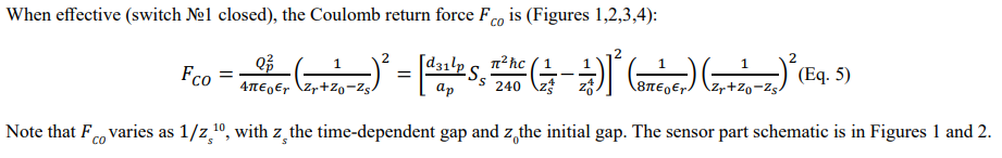
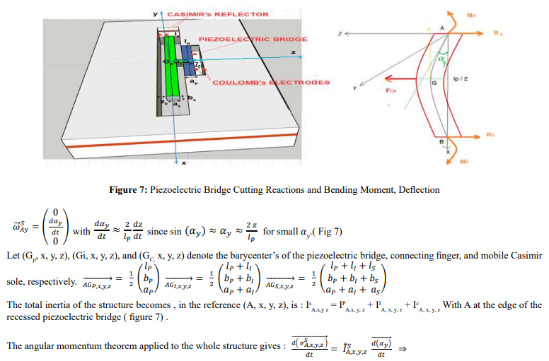
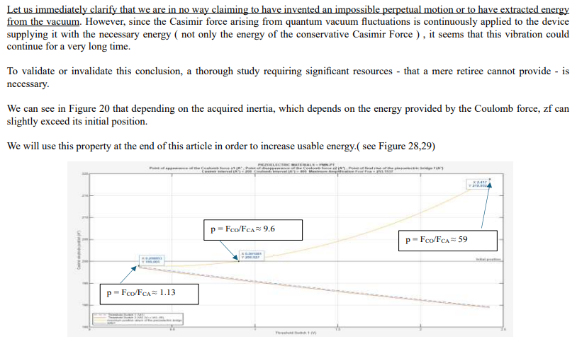
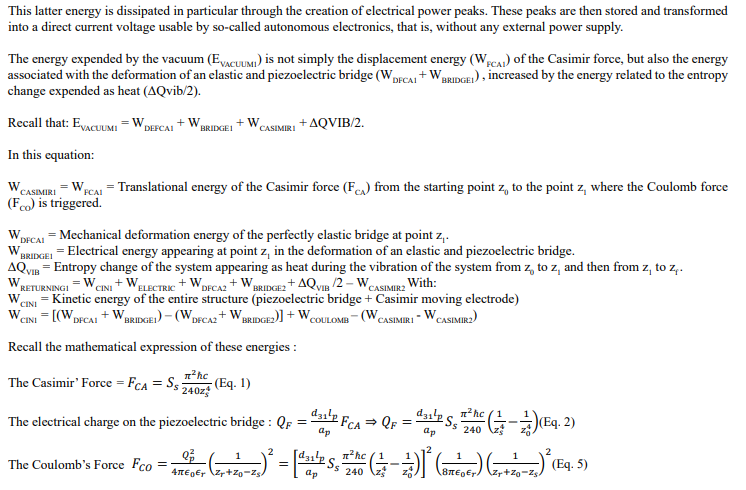
We explore a model where a piezoelectric bridge is deformed by an isotropic, atemporal, attractive Casimir force FCA , and restored by a transient, repulsive Coulomb force FCO induced by the deformation. The schematic of this MEMS is shown in Figures 1 and 2.
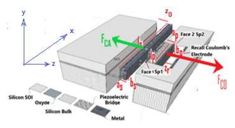
Figure 1:Vue of the Top of Device, Axes, Forces , Casimir’s Electrodes Piezoelectric Bridge Recall Coulomb’s Electrode *ap, bp and lp , are Thickness, Width, and Length of the Piezoelectric Bridge
*ap, bp and lp , are thickness, width, and length of the piezoelectric bridge.
*as, bs and ls , are the thickness, width and length of the Casimir moving electrode.

Figure 2: General Configuration of the Device: MOS Grid Connections (Face 2 of the Piezoelectric Bridge: Red), Source Connections (Face 1 of the Piezoelectric Bridge: Green)
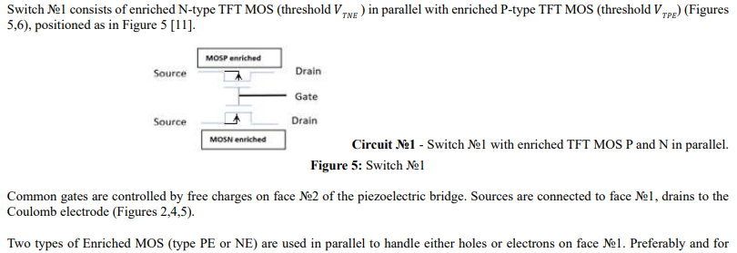
Description of Switches ![]() 1 and
1 and ![]() 2 and Self-contained Passive Switching and Rectification Circuitry
2 and Self-contained Passive Switching and Rectification Circuitry
Switches Electronic Description
Circuit ![]() 1: Switch
1: Switch ![]() 1
1

Circuit ![]() 2: Switch
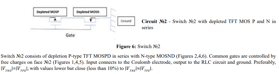
2: Switch ![]() 2
2
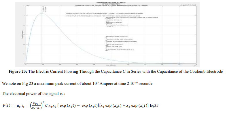
Schematic and Behavior of the MEMS
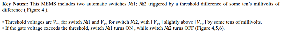
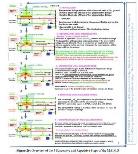
The isotropic and timeless Casimir force, arising from quantum vacuum fluctuations, deforms into a microscopic piezoelectric bridge that is embedded in a silicon wafer (see figures 1 and 2). When switch ![]() 1 is open, mobile charges on face
1 is open, mobile charges on face ![]() 1 remain there ( fig 1,2) . Because an electric field can’t exist in a perfect conductor, when switch
1 remain there ( fig 1,2) . Because an electric field can’t exist in a perfect conductor, when switch ![]() 1 is closed and switch
1 is closed and switch ![]() 2 is open, the electric charges must equalize between face
2 is open, the electric charges must equalize between face ![]() 1 and the Coulomb electrode. If these two electrodes are equal, then charge on the Coulomb electrode is QF/2. Since charges on faces
1 and the Coulomb electrode. If these two electrodes are equal, then charge on the Coulomb electrode is QF/2. Since charges on faces ![]() 1 and
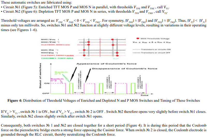
1 and ![]() 2 are opposite, FCO arises. The threshold voltages determine the intensity of the commutation . The Coulomb force FCO can greatly exceed that of FCA. The lifetime of FCO is transient. The disappearance of FCO is determined by the threshold voltages of switch
2 are opposite, FCO arises. The threshold voltages determine the intensity of the commutation . The Coulomb force FCO can greatly exceed that of FCA. The lifetime of FCO is transient. The disappearance of FCO is determined by the threshold voltages of switch ![]() 2. When it switches to ON, the Coulomb electrode is grounded via the R.L.C. circuit which cancels the Coulomb force (Figures 1-6).
2. When it switches to ON, the Coulomb electrode is grounded via the R.L.C. circuit which cancels the Coulomb force (Figures 1-6).
Because Coulomb’s force FCO is much stronger than the Casimir force FCA, the net force FCO - FCA reverses direction. As the piezoelectric bridge deforms less, fewer mobile electric charges are produced, which in turn lowers the gate voltage VG . When Switch ![]() 2 switches to ON and to the mass , the Coulomb force is neutralized. However, the kinetic energy transferred to both the piezoelectric bridge and the mobile Casimir electrode imparts inertia to the structure, which is gradually dissipated due to the ever-present Casimir force FCA. This allows the deformation of the piezoelectric bridge to continue to decrease and return to its initial position (or even slightly exceed it).
2 switches to ON and to the mass , the Coulomb force is neutralized. However, the kinetic energy transferred to both the piezoelectric bridge and the mobile Casimir electrode imparts inertia to the structure, which is gradually dissipated due to the ever-present Casimir force FCA. This allows the deformation of the piezoelectric bridge to continue to decrease and return to its initial position (or even slightly exceed it).
This transient Coulomb force prevents the collapse of the Casimir electrodes and reduces the deformation. The structure returns to initial state or a little above but deforms again under persistent FCA (Figure 2,3).
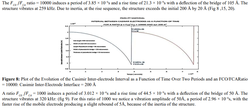
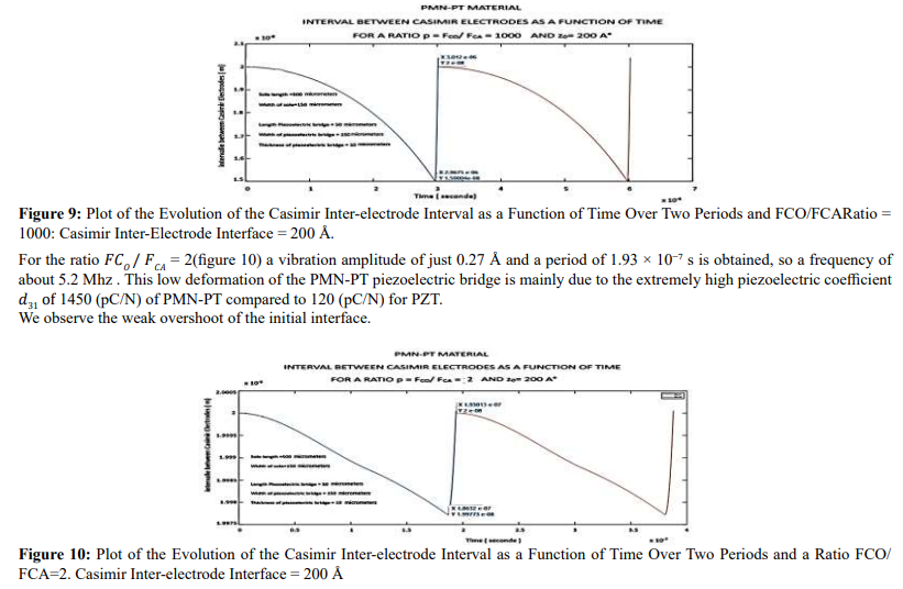
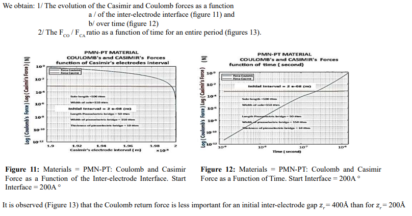
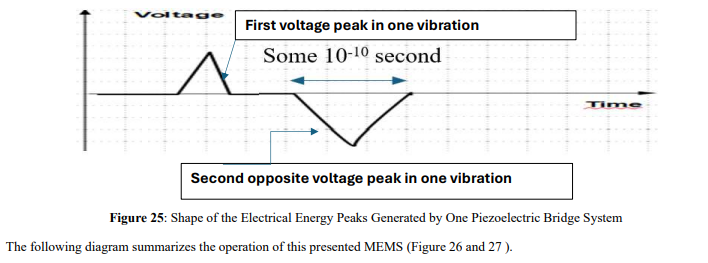
This process may recur, producing vibrations (see Figures 8-10), where Casimir-induced forces, arising from boundary-condition–dependent vacuum fluctuations, act as an effective interaction within the mechanical dynamics of the system. Casimir-induced forces, arising from boundary-condition–dependent vacuum fluctuations, act as an effective interaction within the mechanical dynamics of the system, without implying any active energy source. At each cycle, integrated switches ![]() 1and
1and ![]() 2 redistribute charges on face
2 redistribute charges on face ![]() 1 and
1 and ![]() 2 of piezoelectric bridge .Initially, the Coulomb electrode is grounded by automatic closure of switch
2 of piezoelectric bridge .Initially, the Coulomb electrode is grounded by automatic closure of switch ![]() 2 (Figure 2,4).
2 (Figure 2,4).
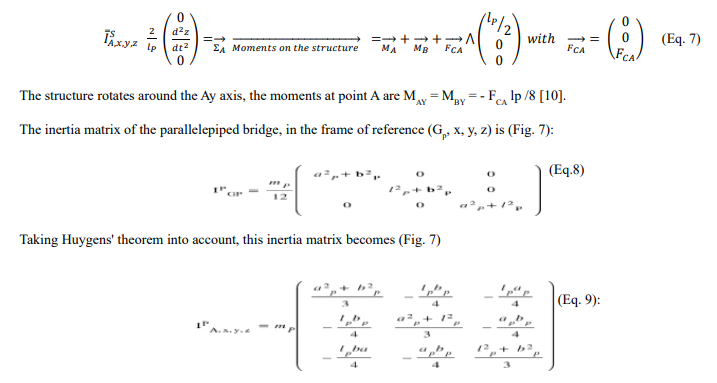
Calculation of the Behavior of the Structure
![]()
Simulation of Devices with Different Piezoelectric Bridge
PMN-PT Piezoelectric Materials for the Piezoelectric Bridge

Evolution of the Casimir Interface as a Function of Time During Two Periods: PMN-PT
Evolution of the Forces of Casimir and Coulomb: PMN-PT
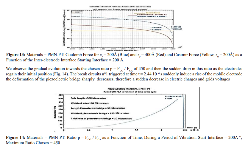
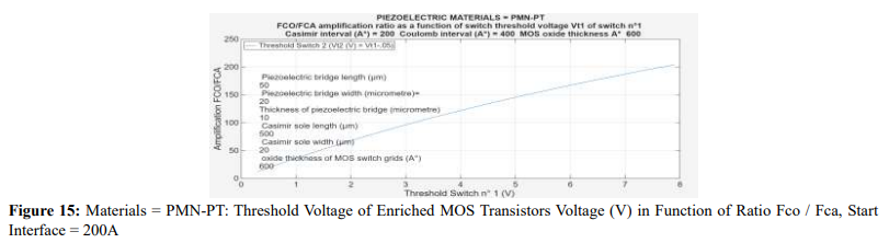
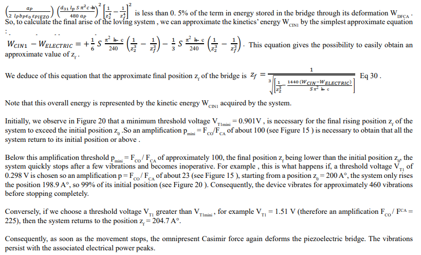
Threshold Voltage According to the Desired Ratio Fco / Fca: PMN-PT
![]()
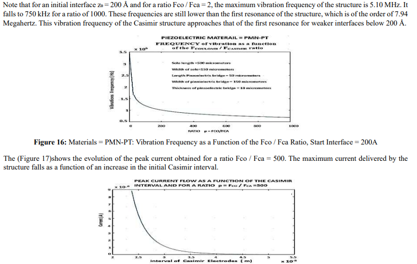
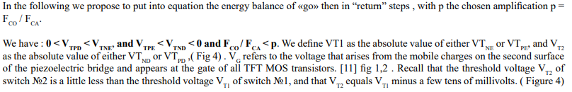
Vibration Frequency as a Function of the Fco / Fca Ratio and Peak Current as a Function of the Initial Casimir Interval Chosen: PMN-PT.

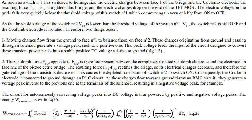
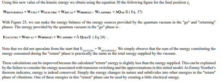
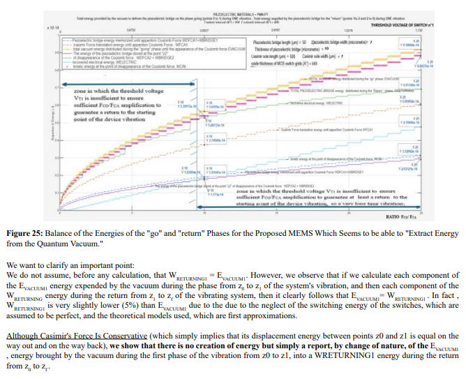
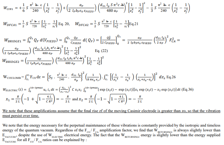
Mems Energy Balance
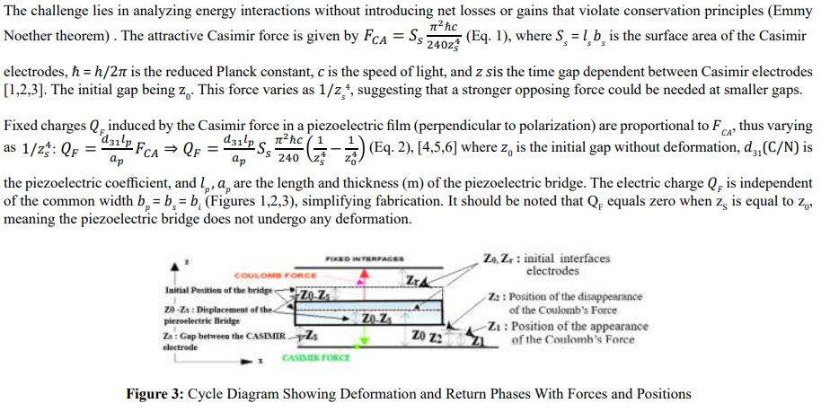
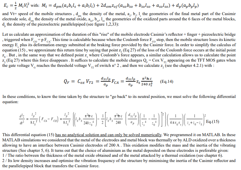
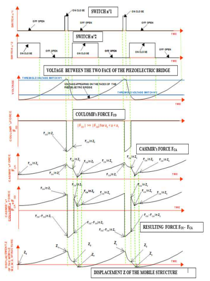
In this part, we will try to make a detailed and exhaustive assessment of the behavior of the MEMS during one vibration. Initially, our attention will be directed towards the initial portion of this vibration, referred to as the "go" phase ( from z0 to z1). Secondly, we will focus on the second half of the vibration, which is to say the "return" phase( Figure 3) . Recall that we assume the piezoelectric bridge is perfectly elastic, meaning any energy used to deform it from position 0 to 1 is fully recovered when returning from 1 to 0. The conditions of use of the piezoelectric bridge (vibrations amplitude) are in the purely elastic domain, and we never enter in the domain of plasticity.
MEMS Energy Balance During the Phase “go” From z0 to z1
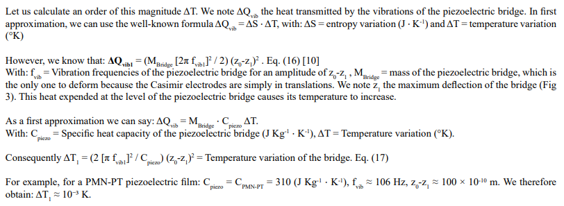
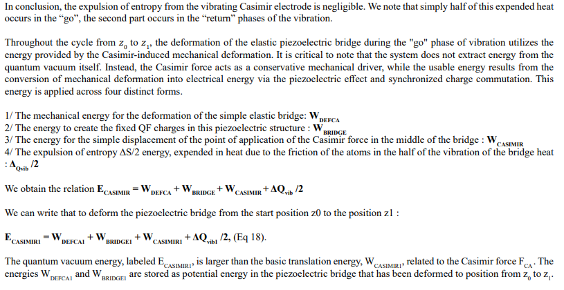
MEMS Energy Balance During the “Return” Phase from z0 to z1” , Switch n°1 ON, Switch n°2 OFF: 0 < abs (VT2) < VG > =abs (VT1 ). and Ratio FCO / FCA> = p: (Figure 1)
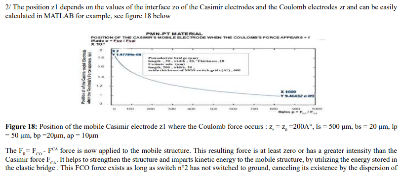
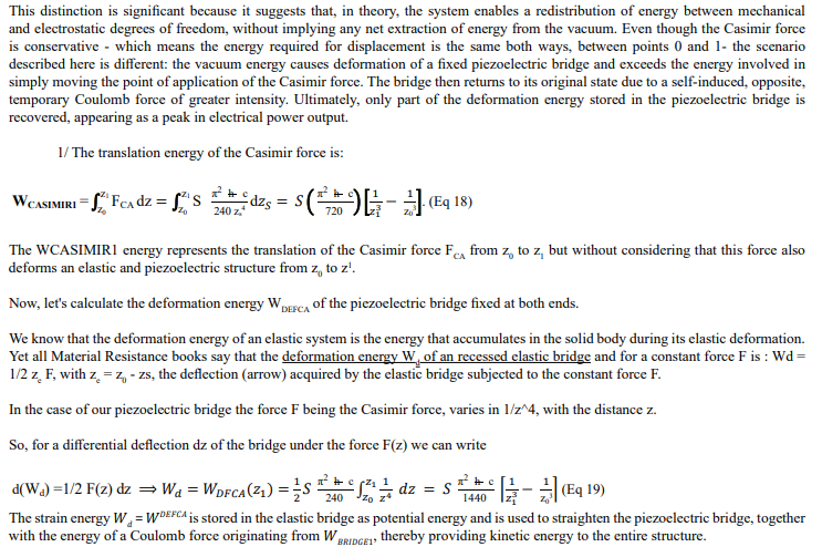
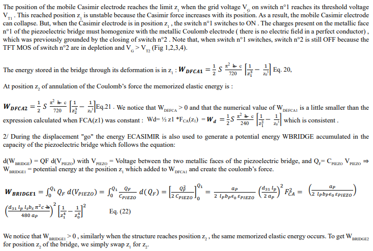
Calculation of Energies Between z1 and z2
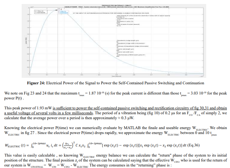
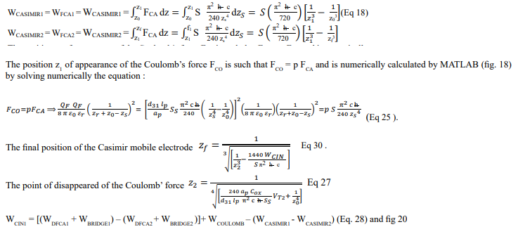
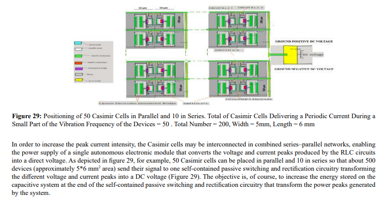
Passive Autonomous Switching Electronics to Transform the Cyclic Power Peaks From the R.L.C. Circuit

Figure 30: Principle of the Single-stage Doubler Without Power Supply Electrical Diagram. All the MOS are Isolated From Each Other by Etching on an S.O.I Wafer, and Their Threshold Voltage is as Close as Possible to Ground
The circuit of the figure 30 is an autonomous device operating without any electrical power source. It rectifies and accumulates the repetitive peak power delivered to the terminals of the RLC circuit in the figure 1 and 2 and transforms them into a usable direct voltage source. The impedance of the output of this autonomous circuit must be important. The results provided by these self-contained passive switching and rectification circuitry are illustrated in the figure 31
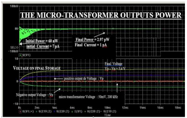
Figure 31: SPICE Simulations of Voltages, Current, Power Consumed by the Self-contained Passive Switching and Rectification Circuitry for the Transformation into Direct Voltage (5.4 V) of an Alternating Input Signal of 50 mV, Frequency = 150 kHz, Number of stages = 14, Coupling Capacities = 20 pF, Storage Capacity = 10 nF
We note the extreme weakness of the electrical power required at the start of the conversion of the power peaks (60 nW) and at the end (2 pW). The conclusions are the same for the electrical current consumption of the transformation electronics, both at the beginning of the transformation (9 pA) and at the end (2 pA). This electrical consumption is significantly lower than what the RLC source can supply. The transformation of the peak of power of 150 kHz , requires about 4 ms.
The interesting points for this presented electronics device are for this SPICE simulation :
1 / the low alternative ( 50 mV) input voltages required to obtain a continuous voltage of several volts at the output
2 / the low power and low current consumed by the source, which in this case is only an RLC circuit, powered by current spikes generated by autonomous vibrations, for this conversion and amplification circuit.
3 / the rapid time to reach the DC voltage (a few ten milliseconds)
The technology used to fabricate the MOSNE and MOSPE transistors of this autonomous electronic, which have the lowest possible threshold voltages, is CMOS on intrinsic S.O.I. and each element is isolated from each other on independent islands. This technology, represented in the following figure 31, strongly limits the leakage currents.
To create these self-contained passive switching and rectification circuitry, we propose using CMOS technology on intrinsic SOI, which isolates each element from the others, thus greatly limiting leakage currents.
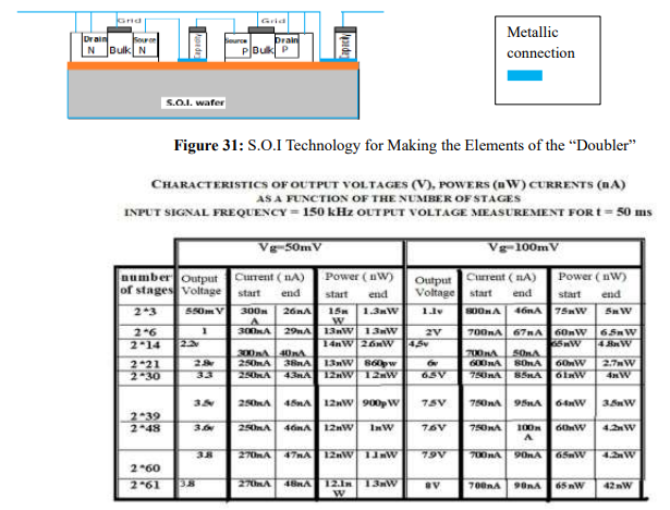
Figure 32: Table 1, Output Continuous Voltage , with Current and Power Consumed by the Autonomous Electronic in Function of Two Input Cyclic Voltage Parametrized with the Number of Stages
We note that the coupling capacities of 20 pF of this electronic, like that of storage of the order of 10 nF, have relatively high values. To minimize the size of these capacitors we propose to use of titanium dioxide as insulator, with a relative permittivity of the order of 100 which is one of the most important for a metal oxide, then the size of the capacity passes to 33 µm for a thickness of TiO2 = 500 Å, which is more reasonable
Technology of Realization of the Current Extractor Device Using the Forces of Casimir in a Vacuum
For the structures presented above, the space between the two surfaces of the reflectors must be of the order of 200 Å, which is not technologically feasible by simply engraving. It seems possible, however, to obtain this parallel space of approximately 200 Å between the Casimir reflectors, not by chemical etching, but by thermal growth or, preferably, by Atomic Layer Deposition (ALD).
Indeed, the Ss3 and Ss2 surfaces of the Casimir reflector must ( figure 1 ,2) :
• be metallic to conduct the mobile charges
• insulating as stipulated by the expression of Casimir's law who established for surfaces without charges.
• This should be possible if we grow an insulator on the z direction of the structure, for example Al2O3 or TiO2 or other oxide metal which is previously deposited and in considering the differences in molar mass between the oxides and the original materials.
For example, silicon has a molar mass of 28 g/mol and silicon dioxide SiO2 of 60 g/mol. It is well known that when silicon dioxide SiO2 grows by one unit, a silicon depth of about 28/60 = 46.6%. This means that the fraction of oxide thickness "below" the initial surface is 46% of the total oxide thickness according to S.M. Sze. [9]
The same must happen, for example for thermal growth of alumina. The molecular masses of Alumina and aluminum are MAl2O3 = 102 g/mole and MAl = 27 g/mole. We obtain an aluminum attack ratio of 27/102 = 26%, which implies that the original surface of this metal has shifted by 26% so that 74% of the alumina has grown out of the initial surface of the aluminum....
As regards the technological manufacture of electronics and structure, it therefore seems preferable:
1 / For electronics to choose Titanium Oxide because of its high relative permittivity εr =114 allowing to minimize the geometries required for the different capacities
2 / For the Casimir structure, the choice of aluminum, because its low density increases the resonant frequency of the structure and that
74% of the Alumina A2O3 is outside the metal, allowing to reduce the interface between Casimir electrodes. A simple calculation shows for example that for aluminum gives...:
If thermal oxidation is used rather the preferred Atomic Layer Deposition, then :
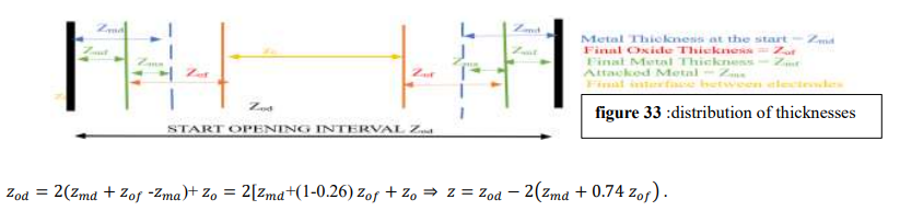
For example, after an opening Zod = 3 μm. We deposit a metal layer of aluminum that is etched leaving a width zmd = 1 μm on each side of the reflector. We then grow a layer of alumina Al2O3 whose thickness is precisely adjusted, simply by considering time, temperature and pressure, in order to obtain the thickness necessary to have the desired z0 interface. For example, if z0 = 200 Å, Zod = 3 μm, zmd = 1 μm, then the grow of AL2O3 on the 1μm of Aluminum is zof = 0.662 μm .The final metallic layer Al remaining will be zmf = 0.338 μm and will act as a conductor under the aluminum oxide.of about 400 A° . So, we obtain a Casimir interface of 200 Å.
Obviously, the growth of this metal oxide between the electrodes of the Casimir reflector modifies the composition of the dielectric present between these electrodes, therefore of the mean relative permittivity of the dielectric. Let: ε0 be the permittivity of vacuum and ε0. εr the metal oxides one (εr = relative permittivity ≈ 8 in the case of Al2O3), zof the final oxide thickness on one of the electrodes and z the thickness of the vacuum present between electrode, (initially we want z = z0).
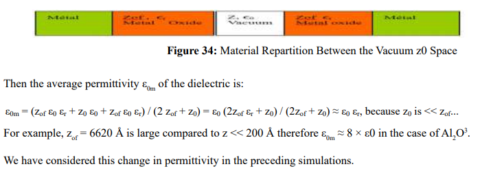
Steps For the Realization of the Structure and its Electronics
We use an SOI wafer with an intrinsic silicon layer : The realization start with voltage "doubler" is obtained by using CMOS technology with 8 ion implantations on an SOI wafer to make :
1. The sources, drains of the MOSNE, MOSND of the "doubler" and of the Coulomb force trigger circuits and of the grounding
2. The source, drains of the MOSPE, MOSPD of the "doubler" and of the Coulomb force trigger circuits
3. Optimally adjust the zero-threshold voltage of the MOSNE in the "doubler" circuit.
4. Optimally adjust the zero-threshold voltage of the MOSPE in the "doubler" circuit.
5. To define the threshold voltage of the MOSNE of the circuit n°1
6. To define the threshold voltage of the MOSPE of the circuit n°1
7. To define the threshold voltage of the MOSND of the circuit n°2
8. To define the MOSPD threshold voltage of the circuit n°2 This electronic done, we take care of the vibrating structure of CASIMIR by :
9. engrave the S.O.I. silicon to the oxide to define the location of the Casimir structures (figure 35)
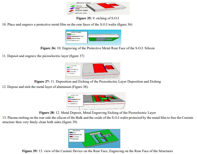
14. After extremely careful cleaning and cutting of the wafer obtained , place the structure in a hermetic integrated circuit support box and carry out all the bonding necessary for the structure to function. After having put the structure in a final box , proceed to the last oxidation under a temperature lower than 150°C of the entire MEMS or preferably by an Atomic Layer Deposition ( ALD) . The thickness of the ALD layer is extremely homogeneous, and ALD deposition is considered perfectly conformal. Under ideal temperature and pressure conditions, with properly chosen parameters, the chemical reactions are complete, thus leaving no impurities in the coating. The coating is dense and exhibits homogeneous, non-columnar growth . The objective is to obtain an adequate Casimir’s and Coulomb’s interface , which is given by the measurement of a adequate voltage obtained at the output of the autonomous transformation electronics.
The in situ electronic circuit should generate a automatic and measurable electrical signal when the interface between the Casimir electrodes becomes weak enough for the device to vibrate and generate a DC voltage, thereby stopping oxidation or ALD deposition.
This voltage measurement indicates that the Casimir and Coulomb effect are effective and automatically controls the end of the oxidation or ALD.
Then the box is closed under neutral gas or vacuum.
This thermal oxidation or ALD after very fine cleaning of the wafer and at the very end of the process makes it possible to control the thickness of the very fine interface between the Casimir and Coulomb electrodes and to oxidize the cleanest possible surfaces without defects. We obtain the device of (Figure 40)
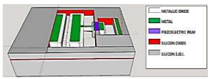
Figure 40: 14. Adjusted Growth of Metal Oxide Front View of the Casimir Device and Coulomb's Electrode, Under Automatic Electronic Control.
15. Create a neutral ambiance or better a vacuum in the hermetic box We remark also that in the case where the 2 metal electrodes of Casimir adhere to one another, they can be separated by the application of an electrical voltage on Coulomb’s electrodes.
Conclusion and Future Perspectives
This work analyzes a nonlinear electromechanical system combining Casimir interactions, elastic deformation, and piezoelectric charge generation within a fully conservative theoretical framework. The proposed model demonstrates that a measurable electrical signal can be generated without any classical external power supply, through the internal redistribution of energy associated with the system’s configuration, including Casimir-dependent boundary conditions.
Part of these repetitive electrical power spikes powers an electronic circuit without any other external power source. The other part is converted into a direct current voltage that evolves in a few milliseconds to a usable voltage of a few volts. The energy consumption of this electronic circuit on these repetitive power peaks is very low.
The Casimir interaction is treated as a configuration-dependent potential energy, constituting an intrinsic part of the system's total Hamiltonian. Variations in this energy, induced by controlled geometric deformation, are redistributed into elastic energy, electrostatic energy, kinetic energy, and dissipative losses, in perfect conformance with the principles of energy conservation and time translation invariance.
No net extraction of energy from the quantum vacuum is claimed. The device is not a self-contained energy source, but rather a nonlinear energy converter capable of transforming internal configuration energy into transient electrical signals. All generated electrical energy is compensated by the corresponding losses, including electromechanical dissipation and electronic imperfections.
It should be noted that an original microtechnology makes it possible to carry out classic CMOS electronics on S.O.I wafers but also, in the last stage, and in a way that is self-controlled by the circuit itself, to define the very small interfaces of the Casimir and Coulomb electrodes, the circuit already being encapsulated.
This study thus clarifies the physical limitations of electromechanical systems assisted by the Casimir interaction, while highlighting their potential interest as demonstrators of energy redistribution mechanisms in nanometric devices, rather than as net power generators.
The system, without requiring a conventional external power supply, redistributes its internal configuration energy into usable electrical signal peaks, which are converted into a usable DC voltage without violating the principle of conservation of energy. The repetitive current peaks provided by the RLC circuit appear sufficient to ensure the transformation, in a few milliseconds, of the periodic signal peaks from the passive RLC circuit into a usable DC voltage of several volts.
We observed that in the referential of our 4 dimensions Space-Time plus the Quantic Vacuum, the energy seems to be conserved which is consistent with Noether’s theorem.
It is important to reiterate that the system does not extract energy from the quantum vacuum but rather harnesses the mechanical work induced by the Casimir force, converting it into electrical energy through the piezoelectric bridge and synchronized charge commutation. This is described as a preliminary result, as the theoretical aspects summarized here have not yet been examined in full detail:
• Neglect of Nonlinearity: The linear dynamic equations do not account for nonlinear electrostatic spring effects or nonlinear material responses, especially at small scales.
• Idealized Joint and Surface Conditions: While the assumption of perfectly flat, mirror-like Casimir plates does not hold true at the nanometer scale, the angstrom-level precision provided by ALD—especially in the final stages of assembly—should enable sufficiently consistent and reproducible resolution.
• Unvalidated Mechanical Model: I was unable to make any comparison with experimental MEMS resonance data or complete 3D FEM models (e.g., from high-fidelity COMSOL or ANSYS simulations).
Piezoelectric Material Selection
The simulations assume ideal material properties, without accounting for thin-film degradation, surface effects, or substrate interactions.
• PZT : Simulations show feasible behavior with moderate current peak output. However, PZT is lead-based, raising environmental and manufacturing concerns.
• PMN–PT :Shows the highest theoretical performance due to a very high piezoelectric coefficient (d31 ≈ 1450 pC/N). However, film deposition at microscale with preserved d31 is technologically nontrivial. The required ~10 µm thick layers are difficult to deposit uniformly while maintaining crystalline orientation and domain structure.
Electrical Conversion Circuit
The energy harvested from the piezo is routed through a MOSFET-controlled switching circuit and then rectified and multiplied using a passive voltage multiplier network. We remark that :
• Efficiency Assumptions: Simulations ignore MOSFET leakage, gate capacitance, threshold variability, and parasitic losses.
• Timing Stability: The concept relies on perfect triggering of MOSFETs based on charge thresholds that are sensitive to temperature and manufacturing variability.
• Lack of Practical Data: No load-line analysis, impedance matching, or power trace simulation is provided.
• No test circuit is presented or fabricated.
Technological Feasibility
The microfabrication scheme (using SOI wafers, etching, sputtering, etc.) is standard in concept, but several issues are overlooked:
• Surface Purity: Any contamination layer (organic films) on Casimir plates suppresses the effect significantly.
• Integration Complexity: Combining PMN–PT films, metal contacts, and active electronics on a single substrate with tight thermal and mechanical tolerances might be complex.
• Switching Timing Precision: The exact timing and response of the electrostatic reset stage relies on transistor thresholds differing by as little as tens of millivolts must be validated .
Physical Realism and Fundamental Objection
• Can vacuum energy actually be extracted? Indeed, within the framework of the dominant quantum field theory, Casimir energy is a potential well, not an energy source.
• Stability of Oscillations: No analysis of long-term stability, phase noise, or stochastic behavior under the influence of vacuum fluctuations has been performed.
• Lack of Empirical Evidence: All claims remain theoretical. I lack the means to build a MEMS prototype for proof-of-concept demonstration to either refute or confirm the conclusions. We believe that, despite the verifications mentioned above, this concept warrants further investigation. The fabrication of a prototype would be the decisive criterion for its confirmation. The theoretical results of this project appear sufficiently encouraging to justify the development of prototypes.
Future Prospects
Several avenues can be explored to advance this work towards experimental realization:
• Fabrication of a MEMS prototype: Using established SOI processes, the central Casimir piezoelectric structure could be fabricated and tested for spontaneous oscillation and charge generation in a vacuum.
• Optimization of the electrostatic tuning mechanism: Improving the design and control of the Coulomb force would allow for precise adjustment of the system's stability point, thus increasing energy production and frequency control.
• Integration with ultra-low threshold CMOS electronics: Coupling the system with high-impedance, low-power electronics would enable the development of autonomous energy harvesting modules for applications in nanometric sensors or space applications.
• Extension to NEMS and 2D material interfaces: Miniaturizing the NEMS architecture and incorporating graphene or MoS2 layers could significantly improve sensitivity to vacuum forces while reducing friction and energy losses.
• Experimental quantification of energy transfer induced by the Casimir effect. Developing precision instruments to measure the net energy extracted over time would help validate the theoretical model and quantify the practical limitations. This work paves the way for a new generation of autonomous microdevices operating at the interface between classical and quantum physics.
This work was carried out entirely by a retired individual. It seems that, barring any errors, Emmy Noether's fundamental theorem of 1905 remains unchallenged.
If theoretical confirmation is obtained by specialists, the creation of a prototype will constitute the ultimate and definitive assessment. If its theoretical predictions are confirmed, it will lead to significant scientific, technological, and human advancements.
This vacuum energy MEMS concept was carried out by an old retiree , completely alone and without the help of any organization As the inventor, I would like to collaborate on their development after signing a contract with the potential investor..
“In the universe, everything is energy, everything is vibration, from the infinitely small to the infinitely large" Albert Einstein. "A person who has never made mistakes has never tried to innovate." Albert Einste
References
- Reynaud, S., Lambrecht, A., Genet, C., Jaekel, M. T. (2001). Fluctuations du vide quantique. Comptes Rendus de l'Academie des Sciences Series IV Physics, 9(2), 1287-1298.
- Casimir, H. B. (1948). On the attraction between two perfectly conducting plates. In Proc. Kon. Ned. Akad. Wet. (Vol. 51, p. 793).
- Lambrecht, A., Reynaud, S. (2000). Casimir force between metallic mirrors. The European Physical Journal D, 8(3), 309-318; Lifshitz, E. M., Pitaevskii, L. P., Berestetskii, V. B. (1980). Landau and lifshitz course of theoretical physics. Statistical physics, Part 2 Ch VIII.
- Deryagin, B. V., Abrikosova, I. I. (1956). Direct measurement of the molecular attraction of solid bodies. 2. Method for measuring the gap. Results of experiments. J. Exp. Theo. Phys., 3, 819-829.
- Vasic, D., Costa, F. (2011). Applications des éléments piézoélectriques en électronique de puissance. Editions TI.
- Wachel, J. C., Bates, C. L. (1976). Techniques for Controlling Piping Vibration and Failures. ASME paper, 76-Pet-18.
- Parasuraman, J., Summanwar, A., Marty, F., Basset, P., Angelescu, D. E., Bourouina, T. (2014). Deep reactive ion etching of sub-micrometer trenches with ultra high aspect ratio. Microelectronic engineering, 113, 35-39.
- Marty, F., Rousseau, L., Saadany, B., Mercier, B., Français, O., Mita, Y., Bourouina, T. (2005). Advanced etching of silicon based on deep reactive ion etching for silicon high aspect ratio microstructures and three-dimensional micro-and nanostructures. Microelectronics journal, 36(7), 673-677.
- Sze, S. M. (2008). Semiconductor devices: physics and technology. John wiley & sons.
- Barthes, M., MECHANICAL, M. C. D. F. S. Vibrational physics. ESTP:(Special School of Public Works).
- Sangouard, P. (1987). Modélisation de transistors polysilicium en couches minces sur isolants: conception et réalisation d'écrans plats à cristaux liquides et matrices actives (Doctoral dissertation, Paris 11).