
Journal of Applied Material Science & Engineering Research(AMSE)
ISSN: 2689-1204 | DOI: 10.33140/AMSE
Impact Factor: 0.98

Research Article - (2025) Volume 9, Issue 1
Novel Electrostatic Spray Deposition (ESD) Techniques for Growth Mechanisms of Solution-Dependent Zinc Oxide (ZnO) Thin Films
2Department of Theoretical Physics, University of Dhaka, Dhaka-1000, Bangladesh
3Department of Electrical Engineering, City Universi- ty, Savar, Birulia, Dhaka, 1216, Bangladesh
4Research Institute, RIST, Tokyo Univ. of Science, Japan
Received Date: Oct 01, 2024 / Accepted Date: Jan 19, 2025 / Published Date: Feb 21, 2025
Copyright: ©Â©2025 Fysol Ibna Abbas, et al. This is an open-access article distributed under the terms of the Creative Commons Attribution License, which permits unrestricted use, distribution, and reproduction in any medium, provided the original author and source are credited.
Citation: Abbas, F. I., Sugiyama, M. (2025). Novel Electrostatic Spray Deposition (ESD) Techniques for Growth Mechanisms of Solution-Dependent Zinc Oxide (ZnO) Thin Films. J App Mat Sci & Engg Res, 9(1), 01-09.
Abstract
In this work, a systematic and easy approach to nanocrystalline (NC) ZnO thin films growth by employing the novel ESD technique at temperatures ranging from 300 °C to 500 °C have been studied. For the subsequent investigation, three sets of 20 ml spray solutions with a 0.1 M concentration of the ESD technique were generated within the laboratory facilities. The solutions contained 80% ethanol (CH3 CH2 OH) and 20% distilled water (H2 O). Zinc chloride (ZnCl2 ) was utilized as the zinc source for all the 20 ml solution. In order to address the fundamental causes of the microstructural changes, two sets of the spray solution were enhanced with hydrochloric acid (HCl) at concentrations of 0.005 M and 0.015 M, respectively. X-ray diffraction (XRD) depictions showed that the ZnO nanoparticles had a pristine wurtzite crystal structure. Energy dispersive X-ray spectroscopy (EDS) and scanning electron microscopy (SEM) showed the composition ratio and growth confirmation of ZnO on the conductive In2O3:Sn (ITiO) coated alkali-free glass substrates. The results show that adding the maximum amount of HCl to the spray solution suppresses the c-axis crystal growth of ZnO thin films and enhance the a-axis (100) crystal growth. The adhesion of anions was believed to be responsible for this suppression. Microstructural parameters (MIP), specifically lattice parameters (a (Å), c (Å)), positional parameters (μ), bond lengths (L (Å)), full width at half maximum (FWHM), and average crystallite sizes (D (nm)), are examined. This finding signifies a pivotal advancement in cost-efficient industrial and commercial applications for ESD-deposited devices.
Keywords
ESD, Thin Film Deposition, ZnO Growth Mechanism, Adhesion, Microstructural Property
Introduction
ZnO nanostructures have been the focus of significant research because their potential for use as a material in various fields, including solar cells, light-emitting diodes, photocatalysis, gas sensors, catalysis, laser diodes, varistors and sensors, is promising [1-9]. ZnO is a widely recognized n-type semiconductor with an enormous band gap of approximately 3.37 (eV) and a substantial exciton binding energy of around 60 (meV) at ambient temperature [10]. However, the use of the methodologies for ZnO nanostructures is restricted due to factors such as elevated temperature, precise gas concentration, hazardous chemical reagents, and expensive equipment. The current goal is to create a simple and cost-efficient method that can be easily expanded for commercial use. Well- established methods for depositing ZnO thin films include dry processes like sputtering and pulsed laser deposition, as well as wet processes like chemical bath deposition, mist chemical vapor deposition, and spray pyrolysis [11-15]. Additionally, the ESD method is not only easy to use, but it also has important industrial benefits, such as the ability to cover large areas because it is simple and easy to understand. This technique allows for non-vacuum deposition, has a low cost, and provides convenient control over the composition ratio and doping [16].
Additionally, this study aims sixfold to investigate the ZnO growth mechanism, and the MIP, namely lattice parameters a (Å), and c (Å)); positional parameters (μ), bond lengths (L (Å)), FWHM, and average crystallite sizes (D), using the novel ESD technology, examining both low concentrations (0.005 M) and comparatively high HCl concentrations (0.015 M) in the prepared spray solution at three different temperatures: 300 °C, 400 °C, and 500 °C, within the framework of precursor solutions dependence on the ITiO glass substrates. Firstly, ESD approach offers not only user-friendly functionality but also significant industrial advantages, including its capacity to effectively cover extensive regions due to its uncomplicated and easily accessible nature. Secondly, this method enables deposition without requiring a vacuum, is reasonable, and offers relatively easy control of the composition ratio and doping. Thirdly, in order to distribute the solution from the metal nozzle edge in ESD, a DC high voltage is positioned between the nozzle and the conductive substrate.
When the flow rate and electric field are adjusted to match the viscosity and resistivity of the solution, the spray shape known as the "cone-jet mode" is illustrated in Figure 1. As the cone-jet mode is engaged in, the droplets that are created are of the same size [13,14]. Fourthly, as the result of the evaporation of the solvent in the droplets, the charge density on the surface of the droplets increases, which results in the droplets automatically splitting apart. Fifth, from the physics point of view, Coulomb forces cause the charged droplets to reject each other, preventing them from colliding. These features allow for the creation of dense and homogeneous thin films using ESD with cover the large area in the ITiO substrate. Sixth, comparing the impact of HCl on the formation of ZnO thin films using the innovative ESD approach.

Figure 1: Schematic Diagram of ESD
The results demonstrate that incorporating the highest concentration of HCl into the spray solution prevents the c-axis crystal formation of ZnO thin films. The weak bonding of anions was thought to be accountable for this suppression. Moreover, few studies have examined the growth mechanism of oxide-based semiconductors deploying the ESD technique and focused on the solution that was selected [15,16]. This work represents a first step in developing cost-effective and easy-to-use technologies that allow visible light to pass through without obstruction using the novel ESD method for oxide-based semiconductor research studies.
Experimental Method
The zinc source utilized in this investigation was zinc chloride (ZnCl2 (98% Assay, ZnCl2=136.32 g), Lot. LEH7398, Mfg. Date. 2021.09, FUJIFILM Wako Pure Chemical Corporation). The solutes were ethanol (CH3CH2OH (99.5%), Cat. No. 14033-70, FW: 46.07, KANTO CHEMICAL CO, INC), and deionized water (H2O). ZnO films were deposited using ESD on a conductive In2O3:Sn (ITiO) coated alkali-free glass substrate. Figure 1 displays the ESD schematic experimental diagram. For the ESD spray method, 20 ml of three (3) different spray solutions were made by changing the molar concentrations of HCl. In order to investigate the growth mechanism of ZnO, nine (9) ITiO substrates have been used with sizes 7.5 mm × 7.5 mm. For preparing the first ESD solution with a 0.1 M concentration, 16 ml of CH3CH2OH was taken in a glass beaker. The density of CH3CH2OH was 0.78945 g/cm3. Next, 0.2726 g ZnCl was added with the CH3 CH2 OH in the glass beaker. To make the solution homogeneous, it was heated for up to 20 minutes in the magnetic stirrer with a hot plate (ADVANTEC SR/350). The temperature was considered 150 oC for the magnetic stirrer with the hot plate. Then 4 ml of H O was added to the solution and heated for 10 more minutes for the uniformity of the solution. A pair of distinct glass beakers were utilized to generate the second ESD spray solution, including 80% CH3CH2OH (16 ml) and 20% H2O (4 ml), respectively. Next, the same amount of ZnCl2 was added to the glass beaker and 16 ml of CH3CH2OH. The same procedure was applied to prepare the homogenous spray solution. Then 4 ml of H2O was poured into the solution containing CH3CH2OH and ZnCl2. The solution mixture was heated for an additional heating period of 10 minutes using a magnetic stirrer with a hot plate. Finally, 0.005 M of HCl was added to the solution and heated for 10 more minutes to ensure the uniformity of the spray solution. In the third ESD spray solution, the sole modification was the addition of 0.015 M HCl and followed the same procedures as the second sample preparation.
ESD spray was performed for 5 minutes at a solution flow rate of 2.0 ml/h on the ITiO substrate surface, and an applied voltage between nozzle and substrate of 8 kV during spraying. During the spraying cycle, the ESD temperature was maintained in the environment at 300 °C, 400 °C, and 500 °C, respectively. The crystallographic orientations of the ZnO films were evaluated using X-ray diffraction (XRD; Rigaku Ultima IV, Rigaku SmartLab). Furthermore, the novel ESD method correlates MIP of the lattice phases. Here, 'a' (Å) represents the lattice parameter along the x-axis, while 'c' (Å) represents the lattice parameter along the z-axis. The lattice positional parameter, μ which is dimensionless parameter, and lattice bond length, L (Å) with the basic crystal growth mechanism [17,18]. The crystallite-growing mechanism of the ZnO thin film was assessed using the Debye-Scherrer equation across several solution frameworks. The relevant sections also addressed the mathematical equations used for this estimation [19- 21].
Result and Discussion
XRD, EDS and SEM Analysis
XRD measurements were carried out for the characterization of the structural properties of the ZnO thin film growth mechanism using the ESD technique for 300 °C, 400 °C, and 500 °C temperatures, respectively. Figure 2 (a-c) represents the XRD pattern of the ZnO thin films on conductive In2O3:Sn (ITiO) coated alkali-free glass substrate. In Figure 2(a), there is a clear, strong peak at the diffraction angle around 34.500 C for the first ESD spray solution sample that doesn't have any HCl mixed in. The solution contains 80% CH3CH2OH and 0.2726 g ZnCl2, with the ZnO thin film at 400 °C, and 500 °C, respectively, mixing with the 20% H2O. Other peaks also appeared for 5000 C temperature (100), (101), (102) plane and those are found weak in crystal orientation respectively, but for 400 °C temperature, (102) plane peak orientation can be seen clearly. (100) and (101) planes were found very weak and no clear visualization. In Figure. 2(a), very weak signal for the crystal phase of (100) plane for the 300 °C temperature was seen, and other crystal phase was not found in fettle mode. Moreover, the consecutive peak appearance for 400 °C, and 500 °C temperature, of the (002) plane in the observation, corroborated the fabrication of ZnO thin films with a hexagonal wurtzite structure [22].
Figure 2 (b) illustrates a prominent peak for the (002) plane at 500 °C, while a very weak peak was noted at 400 °C. The peak strength at 400 °C was inferior to that at 500 °C; furthermore, the peak location at 500 °C migrated somewhat to the left, indicating an increase in the lattice constant along the c-axis at elevated temperatures. The peak strength for the (100) plane was found to be weak at temperatures ranging from 300 °C to 500 °C. The other peak positions corresponding to ZnO thin film growth on the ITIO glass substrate were also observed at the (101) and (102) planes for the 0.005 M HCl mixed ESD spray solution. The ESD sample at 300 °C temperature with this composition showed a very weak but significant peak at the (100) plane of mode.
Figure 2 (c), illustrates the XRD results for a 0.015 M HCl mixed ESD spray solution. The crystal orientation at the (100) plane was significant and was observed consecutively at temperatures of 300 °C, 400 °C, and 500 °C, respectively. Although the peak strength was not very strong, it has a very interesting feature for the high concentration of HCl mixed ESD spray solution. Throughout the entire temperature range under study, a tiny and weak peak emerged at the (101), and (102) planes. Furthermore, in this case, there was no distinct maximum for the (002) plane.

Figure 2: XRD Patterns of ZnO Film According to (a) 0.0 M HCl, (b) 0.005 M HCl, and (c) 0.015M HCl to Weight Ratio of HCl in the Solution Deposited by ESD at 300°C, 400°C and 500°C Respectively
Considering the physical significance of the basic crystal growth mechanism at 400 °C temperature, the development of the crystal growth was observed at the (002) planes, despite the presence of a high concentration of HCl. The fundamental theory of crystal growth determines the growth of ZnO thin films in the c-axis orientation [23]. This theory asserts that the (002) plane of ZnO possesses the lowest surface energy, which plays a crucial role in determining the crystal structure forms. Figure 3(a,b) displayed the results of the EDX and SEM analyses, which confirmed the Zn ration and the homogeneous distribution of particles with a predominantly hexagonal crystal structure during the growth of the ZnO thin film by ESD. Here, the results represent a 0.005 M HCl mixing data, which corresponds to a 500 °C ESD temperature at two different positions on the sample.

Figure 3: SEM and EDS Profile of 0.005 M HCl Mixing in the Solution Deposited by ESD at 500°C Temperature Represent the Confirmation of ZnO Growth and Zn Ratio
Effect of ESD Temperature on Lattice Parameters
ZnO crystallizes in the wurtzite structure, where oxygen atoms are distributed in a, hexagonal close-packed pattern and zinc atoms occupy half of the tetrahedral positions. The Zn and O atoms exhibit tetrahedral coordination with each other, resulting in an identical position. The Zn structure is characterized by an open configuration, where all the octahedral sites and half of the tetrahedral sites are unoccupied. According to Bragg’s law [24].

where n is the order of diffraction (usually n=1), λ is the X-ray wavelength and d is the spacing between planes of given Miller indices h, k and l. In the ZnO hexagonal structure, the plane spacing d is related to the lattice constants a, c and the Miller indices by the following relation [24].
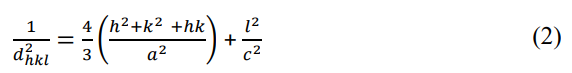
Considering the first-order approximation, n =1, equation (2) can be written:
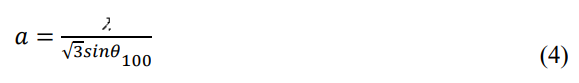
Following the equation (3), the lattice constant, a for the (100) plane is calculated by [17].
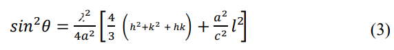
Similarly, for the (002) plane, the lattice constant c is calculated by the equation (3) [17].
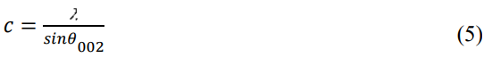
The calculated lattice parameters a (Å), c(Å) and c/a using equation (4) and (5) for this study obtained from ESD is plotted in Figure. 4(a-c), respectively. It is well known that the lattice parameters are temperature dependent, i.e. an increase in temperature leads to expansion of the lattice [19]. In Figure 4. (a), showed the changing effect of lattice parameter, a (Å) for the (100) plane. In the Figure it is seen that without the HCl mixing solution samples, the lattice parameter, a (Å) of the ZnO thin film, is slightly increasing from 300 °C to 400 °C temperature and then it starts to decrease from 400 °C to 500 °C temperature. For the low concentration HCl (0.005 M) mixed ESD samples showed decreasing from 300 °C to 400 °C temperature, and then slightly increasing from 400 °C to 500 °C temperature.
On the other hand, the mixed high-concentration HCl (0.015 M) sample showed a very rigid tendency in its changing mode.Figure 4(b) depicts the changing impact of the lattice parameter, c (Å), on the (002) plane. The picture demonstrates that, in the absence of HCl mixing solution samples, the lattice parameter, c (Å), of the ZnO thin film shows a slight increase from 300 °C to 400 °C, thereafter, decreasing from 400 °C to 500 °C. The low concentration HCl (0.005 M) mixed ESD samples showed an increasing tendency from 300 °C to 500 °C temperature. Moreover,the mixed high concentration of HCl (0.015 M) sample showed decreasing phenomena from 300 °C to 400 °C and increasing from 400 °C to 500 °C temperature. From the physical point of view for the lattice crystal growth, the low-concentration HCl mixed solution showed the systematic increase of lattice tendency on the (002) plane of the ZnO thin film development by the ESD. From the obtained results it can be predicted that the ESD technique is very suitable for the low molar concentration of the lattice development for oxide based thin film technology and the low concentration of HCl result consistent with theory of lattice crystal [23]. The lattice constant ratio is depicted in Figure 4(c), for further analysis.

Figure 4: Structural Parameter Patterns of ZnO Film According to (a) Lattice Parameter, a (Å), (b) Lattice Parameter, c (Å), and (c) Lattice Parameter Ratio, c/a to Weight Ratio of HCl in the Solution Deposited by ESD at 300°C, 400°C and 500°C Respectively
Effect of ESD Temperature on Crystallite and Lattice Bond length
It is known that a perfect crystal would ideally continue infinitely in all directions, but in reality, all crystals are imperfect since they have a limited size [25-27]. The broadening of diffraction peaks in materials occurs due to the deviation from perfect crystallinity. Crystallite size, D (Å) refers to the dimensions of a domain that exhibits coherent diffraction. It is important to note that the crystallite size of particles is typically different from their particle size because of the existence of polycrystalline aggregates. Lattice measure of the distribution is the formulation of lattice constants (a (Å), and c (Å)) arising from crystal imperfections. The X-ray line broadening is used for the investigation of dislocation distribution. In the present study it was found that the ZnO (002) plane diffraction peak is much stronger than the ZnO (101) peak (Figure. 2. (a-c)). This indicates that the formation of ZnO nanocrystals have a preferential crystallographic (002) orientation. The average crystallite size was calculated from XRD peak width of (002) based on the Debye–Scherrer equation,

where β is the integral half width, K is a constant equal to 0.90, λ is the wavelength of the incident X-ray (λ = 0.1540 nm), D is the crystallite size, and θ is the Bragg angle. Figure 5 (a) plotted the estimated average crystallite size, D (nm). The ESD method shows that the ZnO thin film growth mechanism can create the largest value of D (nm) when the HCl mixed spray solution concentration is low. Furthermore, a high concentration of HCl mixed spray solution resulted in a slight decrease in the value of D (nm). In contrast, the absence of the HCl mixed spray solution demonstrated nearly half of the estimated value of D (nm) compared with HCl mixed samples.
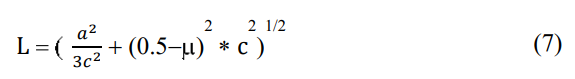
Other MIP μ, and, L (Å) correlated with a (Å), and c (Å) are also studied; and plotted in Figure. 5 (b-c) respectively. The equation has used to estimate the bond length for the ZnO thin films is,
where (µ) is the positional parameter of the wurtzite structure that indicates the extent of atoms displacement relative to the following plane in the c axis, as expressed with
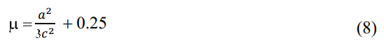
The study of the positional parameter (μ) in the wurtzite structure measures the amount by which each atom gets displaced with respect to the next, and the value of μ can be calculated using Equation (8). Figure. 5 (b) plot the results of μ, representing the without mixed of HCl and mixed of 0.005 M and 0.015 M HCl, respectively. Results for the non-mixing of HCl indicated that the slide increased from 300 °C to 400 °C, and that it decreased from 400 °C to 500 °C temperature. The low HCl mixing results revealed a very rapid decrease from 300 °C to 400 °C and a slight increasing tendency from 400 °C to 500 °C temperature.
However, results for high HCl concentrations showed a slight increase from 300 °C to 400 °C and a decrease from 400 °C to 500 °C temperature. Despite mixing a small amount of HCl (0.005 M), the behavior of this sample remains highly dynamic compared to all the results for μ. This rapidly evolving technique might enable the development of ZnO thin film technology using the ESD approach [21]. In the wurtzite structure, the bond length, L (Å), is determined by measuring the closest distance between atoms in relation to the neighboring atom. The value of L (Å) can be determined using Equation (7). Figure 5 (c) indicates the findings about the lattice bond length, L (Å), of ZnO thin film. The non-mixing HCl results showed a minor temperature increase from 300 °C to 400 °C and a significant temperature decrease from 400 °C to 500 °C at this atomic level. However, for the low concentration, HCl behaves very constant in nature for the (002) plane, which indicates the crystal growth is heavily oriented for this plane and is consistent with the theory of crystal growth mechanism for the ZnO thin film [21]. The non-stable results were also observed for the high concentration of HCl results. From 300 °C to 400 °C it decreases, and from 400 °C to 500 °C temperature it increases. Comparing the results of L (Å) for the three sets of ESD spray solution, very consistent results were found for the low concentration of HCl (0.005 M) mixed sample for the ZnO thin film growth mechanisms.

Finally, ZnO thin films were prepared using the ESD technique. The XRD results in Figure. 2 (a–c) show systematically how a ZnO thin film formed on the conductive ITiO-coated alkali-free glass base. In the absence of HCl and a low concentration of HCl mixing solution, the ZnO thin film crystal orients with the (002) crystal plane. The peak strength significantly decreased as the amount of HCl increased. This is perhaps due to the complex compound formation in the ESD spray solution. The EDX and SEM results showed that the Zn ration and ZnO thin film coexisted on the ITiO substrate. The lattice parameter results showed that low concentrations of HCl mixing ESD have comparable effective data with others. The MIP case study with 0.005 M HCl results also exhibits similar behavior.
After analyzing the current progressive work and the previous work of secondary ion mass spectroscopy data, we proposed the formation of a complex compound of the chloride chemical reaction that occurred in the solution [16]. The excessive presence of the compound element in the solution impedes the growth of the ZnO thin film of the ITiO substrate. Moreover, this proposed chemical reaction mechanism may be effective in the ESD solution due to excessive H2O and other organic compounds. In addition, NC materials inherently contain a certain amount of excess volume in the grain boundaries, and the crystal lattice distortion resulting from the stress field induced by the excess volume is an intrinsic structural characteristic. The experimental work on NC materials indicated that part of the excess enthalpy stored in NC materials originates from distorted crystallites [28]. Further investigation is necessary to elucidate the fundamental process underlying the advancement of thin film technology, thereby ensuring the reaction mechanism and the production of high-quality oxide-based crystals using the ESD approach.

Figure 5: Micro Structural Parameter Patterns of ZnO Film According to (a) Average Crystallite, D (nm), (b) Positional Parameter, μ (dimensionless), and (c) Lattice Bond Length, L (Å) to Weight Ratio of HCl in the Solution Deposited by ESD at 300°C, 400°C and 500°C Respectively
Conclusions
This study found that ESD can develop the oxide-based semiconductor thin film technique cost-effectively. Importantly, future studies on thin-film semiconductor growth mechanisms may apply using the ESD method. Altogether, these findings indicate that employing ESD for depositing the ZnO film is advantageous for creating stacked thin film devices. This work is important as it is the primary stage in developing cost-effective and uncomplicated devices that are transparent to visible light using the ESD method for semiconductor oxide-based materials. It also aims to investigate the ZnO growth process using ESD.
Acknowledgements
The authors express their sincere appreciation to Mr. Keisuke Tomono, Mr. Keito Okubo, and Mr. Kohta Hori for their support in completing the experiments and for the constructive discussions.
Funding
This work was sponsored by MEXT for the scholarship of supporting international student (Fysol Ibna Abbas), JSPS KAKENHI (Grant number: 21K04696), and the Renewable Energy Science and Technology Research Division of the Tokyo University of Science.
Conflict of interest
The authors of this work declare that they have no conflicts of interest.
References
- Bitenc, M., & Orel, Z. C. (2009). Synthesis and characterization of crystalline hexagonal bipods of zinc oxide. Materials Research Bulletin, 44(2), 381-387.
- Choi, Y. S., Kang, J. W., Hwang, D. K., & Park, S. J. (2009).Recent advances in ZnO-based light-emitting diodes. IEEE Transactions on electron devices, 57(1), 26-41.
- Baruah, S., & Dutta, J. (2009). Hydrothermal growth of ZnO nanostructures. Science and technology of advanced materials, 10(1), 013001.
- Dolabella, S., Borzì, A., Dommann, A., & Neels, A. (2022). Lattice strain and defects analysis in nanostructured semiconductor materials and devices by high-resolution Xray diffraction: Theoretical and practical aspects. Small Methods, 6(2), 2100932
- Zhu, L., & Zeng, W. (2017). Room-temperature gas sensing of ZnO-based gas sensor: A review. Sensors and Actuators A: Physical, 267, 242-261.
- Alim, K. A., Fonoberov, V. A., & Balandin, A. A. (2005). Origin of the optical phonon frequency shifts in ZnO quantum dots. Applied Physics Letters, 86(5).
- Tennyson, E. M., Doherty, T. A., & Stranks, S. D. (2019). Heterogeneity at multiple length scales in halide perovskite semiconductors. Nature Reviews Materials, 4(9), 573-587.
- Ram, S. G., Ravi, G., Athimoolam, A., Mahalingam, T., & Kulandainathan, M. A. (2011). Aqueous chemical growth of free standing vertical ZnO nanoprisms, nanorods and nanodiskettes with improved texture co-efficient and tunable size uniformity. Applied Physics A, 105, 881-890.
- Ada, K., Gökgöz, M., Önal, M., & Sarikaya, Y. (2008). Preparation and characterization of a ZnO powder with the hexagonal plate particles. Powder Technology, 181(3), 285- 291.
- Thomas, D. G. (1960). The exciton spectrum of zinc oxide.Journal of Physics and Chemistry of Solids, 15(1-2), 86-96.
- Nakai, H., Sugiyama, M., & Chichibu, S. F. (2017). Ultraviolet light-absorbing and emitting diodes consisting of a p-type transparent-semiconducting NiO film deposited on an n-type GaN homoepitaxial layer. Applied Physics Letters, 110(18).
- Dutta, T., Gupta, P., Gupta, A., & Narayan, J. (2010). Effect of Li doping in NiO thin films on its transparent and conducting properties and its application in heteroepitaxial pn junctions. Journal of Applied Physics, 108(8).
- Xia, X. H., Tu, J. P., Zhang, J., Wang, X. L., Zhang, W. K., &Huang, H. (2008). Morphology effect on the electrochromic and electrochemical performances of NiO thin films. Electrochimica Acta, 53(18), 5721-5724.
- Tomono, K., & Sugiyama, M. (2024). Investigating electrical properties and crystal growth in NiO thin films by spray pyrolysis and electrostatic spray deposition. Japanese Journal of Applied Physics, 63(2), 025504.
- Cullity, B. D. (1956). Element of X-Ray Diffraction. Upper Saddle River: Prentice Hall.
- Abbas, F. I., & Sugiyama, M. (2024). Solution-dependent electrostatic spray deposition (ESD) ZnO thin film growth processes. arXiv preprint arXiv:2406.13313.
- Pope, C. G. (1997). X-ray diffraction and the Bragg equation.Journal of chemical education, 74(1), 129.
- Pal, U., Serrano, J. G., Santiago, P., Xiong, G., Ucer, K. B.,& Williams, R. T. (2006). Synthesis and optical properties of ZnO nanostructures with different morphologies. Optical Materials, 29(1), 65-69.
- Saleem, M., Fang, L., Ruan, H. B., Wu, F., Huang, Q. L., Xu, C. L., & Kong, C. Y. (2012). Effect of zinc acetate concentration on the structural and optical properties of ZnO thin films deposited by Sol-Gel method. Int. J. Phys. Sci, 7(23), 2971-2979.
- Bindu, P., & Thomas, S. (2014). Estimation of lattice strain in ZnO nanoparticles: X-ray peak profile analysis. Journal of Theoretical and Applied Physics, 8, 123-134.
- Kumar, V., Sharma, H., Singh, S. K., Kumar, S., & Vij, A. (2019). Enhanced near-band edge emission in pulsed laser deposited ZnO/c-sapphire nanocrystalline thin films. Applied Physics A, 125, 1-7.
- Singh, S. K., & Singhal, R. (2018). Thermal-induced SPR tuning of Ag-ZnO nanocomposite thin film for plasmonic applications. Applied Surface Science, 439, 919-926.
- Raoufi, D. (2013). Synthesis and microstructural properties of ZnO nanoparticles prepared by precipitation method. Renewable Energy, 50, 932-937.
- Uno, K., Yamasaki, Y., & Tanaka, I. (2016). Growth mechanisms of zinc oxide and zinc sulfide films by mist chemical vapor deposition. Applied Physics Express, 10(1), 015502.
- Dommann, A., & Neels, A. (2009). The role of strain in new semiconductor devices. Advanced Engineering Materials, 11(4), 275-277.
- Bardeen, J., & Shockley, W. J. P. R. (1950). Deformation potentials and mobilities in non-polar crystals. Physical review, 80(1), 72.
- Dunne, F. P. E., Kiwanuka, R., & Wilkinson, A. J. (2012). Crystal plasticity analysis of micro-deformation, lattice rotation and geometrically necessary dislocation density. Proceedings of the Royal Society A: Mathematical, Physical and Engineering Sciences, 468(2145), 2509-2531.
- Abbas, FI., & Sugiyama M. (2024). Investigation the anisotropic feature using structural and mechanical profile analysis of Zinc Oxide (ZnO) thin film growth mechanism within the framework of williamson-hall estimation by novel Electrostatic Spray Deposition (ESD) technique. Journal of Physics: Applications and Mechanics;1(1):1005.