
Current Research in Environmental Science and Ecology Letters(CRESEL)
ISSN: 2997-3694 | DOI: 10.33140/CRESEL


Research Article - (2024) Volume 1, Issue 2
Electronic Properties of (B) GaAs/GaAs Heterostructure Capped by Ga2O3
2Institut Supérieur des Sciences Appliqués et Technologie de Sousse, Université de Sousse, Tunisia
Received Date: Feb 03, 2024 / Accepted Date: Jun 25, 2024 / Published Date: Jul 04, 2024
Copyright: ©Â©2024 Faouzi Saidi, et al. This is an open-access article distributed under the terms of the Creative Commons Attribution License, which permits unrestricted use, distribution, and reproduction in any medium, provided the original author and source are credited.
Citation: Slimi, D., Saidi, F., Maaref, H. (2024). Electronic Properties of (B)Gaas/Gaas Heterostructure Capped by Ga2O3. Curr Res Env Sci Eco Letters, 1(2), 01-10.
Abstract
In this work we performed optical studies of Ga2 O3 /GaAs, BGaAs/GaAs and Ga2 O3 /BGaAs/GaAs epilayers obtained by chemical vapor deposition (MOCVD) at different growth temperatures (580°C and 670°C). This enables the development of heterostructures based on BGaAs/GaAs thin films covered by Ga2 O3 . We focused our research on the influence of power excitation and temperature on the photoluminescence (PL) properties. Ithasshowedthe presence of emission energy around 1.2 eV and a red shift after the deposition of Ga2 O3 on BGaAs/GaAs at low temperature (10K). The power study highlights the dominance of the Ga2 O3 layer during the emission via the donor-acceptor transitions. The evolution of the emission energy temperature for the BGaAs/GaAs thin film allowed us to explain the origin of the excitonic recombination. The luminescence within the new Ga2 O3 /BGaAs/GaAs heterostructure is controlled by the localization of carriers in energy fluctuation potentials created by inhomogeneous distributions of VGa families. We have shown that this proposed heterostructure based on III-V semiconductors could broaden the emission spectrum and henceincreasestheconversion efficiency as the absorption increases.
Keywords
GaAs, BGaAs, Ga2O3, MOCVD, PL
Introduction
Right now, III-V semiconductor materials based on GaAs, InAs (BAs) and their ternary alloys BxGa1-xAs (InxGa1-xAs) are favored for their potential use in photonic, electronic and optoelectronic devices such as blue light emitting diodes and green high electron mobility transistors (HEMT) and metal oxide semiconductor capacitors (MOSCAP) diode lasers thin-film solar cells Electrooptic waveguide modulators metal-insulator- semiconductor photodetectors [1-10].
In fast electronics and optoelectronics, as silicon has been well developed and commercialized in the photovoltaic field due to its high absorbance, abundance and low cost, it remains insufficient in the optoelectronic field and more precisely for the design of transmitters due to the low mobility of the carriers and its indirect gap which reinforces the non-radiative transitions. On the other hand, III-V semiconductors are favored by their direct gap, their high mobility and their high electrical conductivity [11]. The main efforts have been undertaken to develop new photovoltaic conversion routes based on III-V semiconductors such as GaAs, In ... etc. [12].
Moreover, they are materials of choice for the development of lasers or detectors operating in the telecommunication domain at wavelengths of 1.3μm [13]. In this context, our mastered heterostructure is based on the III-V semiconductors Ga2O3/ BGaAs/GaAs. The latter generates a new structure applicable in optoelectronics emitting in the 1.3-1.55 micrometer range [12]. The choice of GaAs as substrate due to its high carrier confinement in the active region, its infrared emission and its low cost [14]. The introduction of Boron in GaAs has allowed to decrease the emission energy compared to GaAs and reach the wavelength 1.33 micrometer [15]. Indeed, it acts on the state of strain but it is limited by the incorporation of boron we cannot reach concentrations < 8% this is accompanied by the presence of energy levels in the band gap generally related to boron aggregates (clusters) [16,17]. The advantage of adding Ga2O3 is that it broadens the emission range since it emits in the UV range and is a transparent conductive material [18]. From an energy point of view, these materials have a different energy diagram. In fact,these three semiconductors are distinguished by their band gaps which are 1.42 eV for GaAs, 1.34 eV for BGaAs and 4.6_ 4.9 eV for Ga2O3 [19,20]. In this heterostructure we find energy levels below the BC of BGaAs. Gallium oxide also has deeper energy levels in its optical gap at energies of 2.4, 2.75, 3 and 3.15 eV [21]. These different gap energies make a richness for us in terms of optoelectronic applications.
Experimental Details
The heterostructure we studied consists of a GaAs substrate, a buffer layer on which a thin layer of BGaAs is deposited, a gallium arsenide barrier followed by a gallium oxide Ga2O3layer. The samples are grown by MOCVD in a horizontal T-shaped reactor at atmospheric pressure [22-24]. GaAs exhibits a 1° disorientation from the (001) plane in the [110] direction. Triethylgallium (TEG) and diborane (B2H6) are used as group III precursors for gallium (Ga) and boron (B), respectively. Arsine (AsH3) is used as group V precursor for arsenic (As). All the growths of these structures took place under hydrogen, which is the carrier gas used in EPVOM. Photoluminescence measures were performed between 10 and 300K by holding the samples in an unrestricted cycle helium cryostat. The sample was excited by the green line (wavelength 514.5 nm) of an argon-ion laser (Ar+) with a maximum power density of 80 W/cm². Photons emitted by the sample are scattered by a high-resolution spectrometer (Jobin-Yvon monochromator HDR1: focal length 0.6). Detection is via a silicon detector (spectral range between 800 and 1200 nm) with integrated amplifier.
Results and Discussion
Figure 1 show that the low temperature PL spectrum of GaAs has a sharp emission peak at 1.516 eV [24,25]. When depositing Ga2O3/ GaAs, we observe that the emission energy at 1.43eV red shifted by 80meV compared to GaAs dominate the GaAs PL emission peak. This shift may be a consequence of the excess of carbon concentration since the deposition was done by MOCVD [26].

Figure 1: Room Temperature PL Spectrum for Ga2O3/GaAs.
To confirm the nature of this heterostructure, PL measurements are performed at 10K and under different excitation power densities on Ga2O3/GaAs (see Figure 2).

Figure 2: Shows the Low Temperature Photoluminescence PL Spectra of Ga2O3 Grown on GaAs
Indeed, as the excitation power increases, the intensity increas- es as well as the full width at half maximum. Moreover, a small blue energy shift is observed in the 10 - 100 mW excitation power range. From this power study, we can see that this heterostructure is of type I [27]. In order to clarify the PL transition medium, the analysis of PL intensity as a function of the excitation density is performed. A power law fitting allowed determining the nature of this transition as shown in Figure 3. This law is given by the fol- lowing expression:

Where IPL is the PL intensity, PðÂÂ??ðÂÂ?? is the excitation power, and n is the dimensionless exponent which can take the following forms [27]. • n ≤ 1: Recombination from the free state to the bound state or from the bound state to another bound state.
• n = 1: Band to band recombination.
• 0< n< 1: Excitonic recombination.

Figure 3: PL Intensity as a Functions of Exciter Power for Ga2O3/Gagas Heterostructure
In our structure n= 0, 7: the type of recombination is a transition from the donor state to the acceptor state (D-A), which has already been proven by the work of R. Fornari in which the excitation is done by cathodoluminescence with an energy varying between 5 and 30 KeV [21]. Figure 4 shows the different spectra of the Ga2 O 3/GaAs sample by varying the temperature from 10 to 300 k. An increase in PL inten- sity and width at half maximum is detected in the range of 10 to 60 K. For T<60 K, a drop in PL intensity while increase in LWHM is marked this and justified by the PL intensity ratioI I10 ~10 which I300 shows that this reflects a strongly present non-radiative character due to defects and impurities.
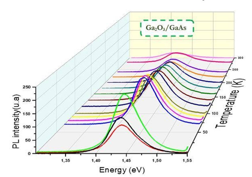
Figure 4: PL Spectra at Different Temperatures of the Ga2O3/GaAs Layer
In order to confirm and validate the presence of the localization phenomenon, we studied the variation of the energy position of the photoluminescence peak as a function of the temperature of the Ga2O3/GaAs epilayers (see Figure 5). These spectra could be adjusted by the empirical law proposed by Varshni using Equation (1) [28,29].
Where Eg(0) is the energy of the gap at T=0 K, α is an empirical parameter related to the joint density of states and β an effective tem- perature. By fitting the experimental results with
Equation (1), we have deduced the different values of α and β shown in Table.
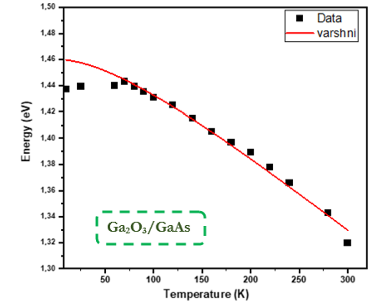
Figure 5: The Evolution of PL Energy as a Function of Temperature
|
Sample Name |
α (ev/K) 10-4 |
β(K) |
Eg(0) (eV) |
|
Ga2O3/GaAs |
6,159 |
125 |
1,46 |
|
BGaAs/GaAs |
5,969 |
168 |
1,343 |
Table: Varshni parameter of Ga2 O 3/GaAs and BGaAs grown at 670 oC and 580 oC for Boron Composition Xb = 1.5%, Respec-tively
At low temperature, Varshni's law does not correspond to the ex- periment given for the Ga2O3/GaAs epilayer. It exhibits an anom- alous behavior, the so-called S-shape. From 10 to 70 K the emis- sion energy increases, but a decrease is observed between 70 and 100 K. This shape is a signature of the localization phenomenon, which can be related to localized states in the Ga2O3 layer. At high temperature, no distinction can be observed between the expected Varshnienergy band gap and the PL energy peak because the car- riers are thermally delocalized and one joins the evolution guided by band-to-band recombination; this behavior can be attributed to the emission of GaAs.
After studying the Ga2O3/GaAs reference structure, we now pro- ceed to the characterization of the Ga2O3/BGaAs/GaAs hetero- structure to compare the effect of boron and gallium oxide on GaAs. To compare the optical properties of BGaAs/GaAs layer sand Ga2O3/BGaAs/GaAs heterostructures, we first demonstrate low-temperature photoluminescence spectra. For the BGaAs/GaAs layer (Figure 6a), PL emission from GaAs substrates is dominated by the carbon impurity transition (e-CAs) and its phonon-optical replica (LO) [30]. In addition, an asymmetric PL band named (HE) centered at 1.334 eV with a half-value width of 89 meV has been reported. This emission band is associated with exciton recombi- nation of BGaAs [13]. When the gallium oxide layer is deposited on BGaAs/GaAs, a broad peak centered around 1.20 eV with a full width at half maximum of 185 meV is observed (see Figure 6b). Thus, we notice that after the deposition a broader emission peak is observed with an increase in the full width at half maxi- mum. Figure 7 shows PL spectra at different powers of the BGaAs/ GaAs structure and of the Ga2O3/BGaAs/GaAs heterostructure performed at low temperature and with an excitation wavelength equal to 514.5 nm (Xb=1.5%). For both structures, we observe that when we increase the excitation power, the PL intensity increases with increasing full width at half maximum.

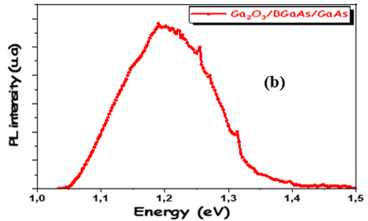
Figure 6: PL Spectra at 10K: of the BGaAs/GaAs Layer (A) and of the Ga2O3/BGaAs/GaAs Heterostructure (B).
From Figure 7a, we observe a broadening of the PL peak of BGaAs. This is due to the gradual filling of the energy levels introduced by boron in the GaAs gap. Moreover, Figure 7b shows that the broad luminescent band is shifted towards the low energy. Indeed, this important shift towards high wavelengths is related to the gradual filling of energy levels introduced by the Ga2O3 oxide deposited on the BGaAs layer.

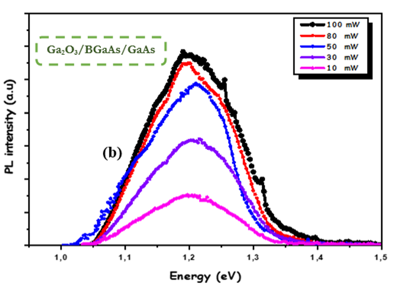
Figure 7: PL Spectra at Different Excitation Powers: of the BGaAs/GaAs Structure (A) and of the Ga2O3/BGaAs/GaAs Hetero- structure (B)
In the same framework, the evolution of the PL intensity as a func- tion of the exciter power is shown for the Ga2O3/BGaAs/GaAs het- erostructure (see Figure 8). A power law fitting has allowed us to determine the coefficient n which proves that the transition is of donor-acceptor type since n<1 (n=0.5). This n is comparable with the one found by Roberto and his collaborators [20].

Figure 8: PL Intensity as a Function of Exciter Power for Ga2O3/BGaAs/GaAs Heterostructure
In order to deeply understand the recombination mechanisms of the Ga2O3/BGaAs/GaAs heterostructure we have performed a study of the PL intensity as a function of temperature. From this study, we observe that the PL intensity increases with temperature and then decreases. Moreover, we notice that the full width at half maximum is also increasing with temperature. However, for low temperatures we have an energy shift towards the blue and a shift towards the red of the energy peak from the temperature 50 K (see Figure 9).

Figure 9: PL Spectra of the Ga2O3/BGaAs/GaAs Sample at Different Temperatures
For the Ga2O3/BGaAs/GaAs heterostructure, the peak is very broad and we could not follow the evolution of energy, intensity and full width at half maximum as a function of temperature. Whereas for the BGaAs/GaAs epilayer, Figure 10 shows the temperature de- pendence of the PL band energy which gives a good fit according to Varshni's laws (Equation (1)). We have a good correlation be- tween the results of the experiment and the Varshni adjustment. Moreover, the difference ΔE (10 K) between the measured PL peak energies and the expected transition energies at 10 K (obtained by simulating the measured temperature dependence of the PL peak positions by the well-known Varshni relation) are suggested to be related to Stokes shifts, is about 5 meV, may be due to the recom- bination of photogenerated carriers trapped by localized states in BGaAs [23,30]. Indeed, it exhibits anomalous behavior, the so- called S-shape between 10 and 90 K. This shape is the result of carriers jumping between localized states created by boron clusters [31]. At high temperature, the PL band is similar to the variation of the energy band gap. This indicates that the carriers acquire more thermal energy to reach the conduction band. They relax giving rise to band-to-band recombination [25-31].

Figure 10: The Evolution of PL Energy as a Function of Temperature
Conclusion
In summary, the study of optical properties by steady-state photo- luminescence of the active layer shows that there is an emission and red shift of about 1.2 eV after low temperature deposition of Ga2O3 on BGaAs/GaAs. However, performance studies highlight the dominance of the Ga2O3 layer in the emission process of the donor-acceptor transition. Boron segregates in the direction of the Ga2O3 layer, resulting in a reduction in boron content and a reduc- tion in tensile stress, resulting in a reduction in the layer. The study of PL as a function of temperature on BGaAs/GaAs structures leads us to conclude that the observed luminescence is the origin of exciton recombination, which is associated with discrete states formed by the aggregation of boron atoms under band gap condi- tions. The luminescence in the new Ga2O3/BGaAs/GaAs structure is governed by the localization of charge carriers in the energy fluctuation potential created by the inhomogeneous distribution of the VGa family.
Data Availability Statement
We confirm that all data presented in the paper are original and realized in our laboratory by the authors.
Authors Contribution Statement
We are pleased to submit an original research article entitled “Op- tical properties of Ga2O3 deposited on (B)GaAs/GaAs heterostruc- tures for optoelectronic application”. The results presented is this paper were carried out in our lab by the authors: Dalanda Slimi, Faouzi Saidi, and Hassen Maaref, submitted for possible publica- tion in this journal. We confirm that all authors contributed equally to the paper.
References
- Steiger Wald, D., Rudaz, S., Liu, H., Kern, R. S., Götz, W., & Fletcher, R. (1997). III–V nitride semiconductors for high-performance Blue and green light-emitting devises. Jom, 49, 18-23.
- Li, H., Wu, J., Wang, Z., Liang, J., Xu, B., Jiang, C., ... & Zhou, W. (1998). Growth and characterization of InGaAs/In- AlAs/InP high-electron-mobility transistor structures towards high channel conductivity. Journal of crystal growth, 186(3),309-314.
- Nguyen, N., Jiang, Z., Forgie, K., Nam, W. J., Xu, J., et al. (2013). Electron Dev. 60(1), 235-240.
- Hadjab, M., Berrah, S., Abid, H., Ziane, M. I., Bennacer, H., & Yalcin, B. G. (2016). Full-potential calculations of struc- tural and optoelectronic properties of cubic indium gallium arsenide semiconductor alloys. Optik, 127(20), 9280-9294.
- Lee, A., Liu, H., & Seeds, A. (2012). Semiconductor III–V lasers monolithically grown on Si substrates. Semiconductor science and technology, 28(1), 015027.
- Dimroth, F. (2006). High-efficiency solar cells from III-V compound semiconductors. physica status solidi c, 3(3), 373- 379.
- Cotal, H., Fetzer, C., Boisvert, J., Kinsey, G., King, R., He- bert, P., ... & Karam, N. (2009). III–V multijunction solar cells for concentrating photovoltaics. Energy & Environmental Sci- ence, 2(2), 174-192.
- Wu, K., Tong, C. Y. E., & Vahldieck, R. (1991). Microwave characteristics of high-speed traveling-wave electrooptic modulators on III-V semiconductors. Journal of lightwave technology, 9(10), 1295-1304.
- Remiens, D., Pribetich, P., Kennis, P., & Seguinot, C. (1987). Microwave performance prediction of a III–V semiconductor electrooptic waveguide modulator. Applied optics, 26(1), 118- 120.
- Brouckaert, J., Roelkens, G., Van Thourhout, D., & Baets,R. (2007). Thin-film III-V photodetectors integrated on sili- con-on-insulator photonic ICs. Journal of Lightwave Technol- ogy, 25(4), 1053-1060.
- Tarbi, A., Chtouki, T., Bouich, A., ElH.,…& Aissat, A. (2022). Optical Materials. 131, 112704.
- Hamila, R., Saidi, F., Rodriguez, P. H., Auvray, L., Monteil, Y., & Maaref, H. (2010). Growth temperature effects on boron incorporation and optical properties of BGaAs/GaAs grown by MOCVD. Journal of alloys and compounds, 506(1), 10- 13.
- Mehdi, H., Réveret, F., Robert-Goumet, C., Bideux, L., Gruz- za, B., ...& Monier, G. (2022). Applied Surface Science, 579, 15219.
- Szwacki, N. G., & Bogus-awski, P. (2001). GaAs: N vs GaAs: B alloys: Symmetry-induced effects. Physical Review B, 64(16), 161201.
- Boguslawski, P., & Gorczyca, I. (1994). Atomic-orbital in- terpretation of electronic structure of III-V semiconductors: GaAs versus AlAs. Semiconductor science and technology, 9(12), 2169.
- Ilahi, S., Baira, M., Saidi, F., Yacoubi, N., Auvray, L., & Maaref, H. (2013). Non-radiative recombination process in BGaAs/GaAs alloys: Two layer photothermal deflection mod- el. Journal of alloys and compounds, 581, 358-362.
- Parisini, A., Bosio, A., Montedoro, V., Gorreri, A., Lamperti, A., Bosi, M., ... & Fornari, R. (2019). Si and Sn doping of ε-Ga2O3 layers. APL Materials, 7(3).
- Geisz, J. F., Friedman, D. J., Olson, J. M., Kurtz, S. R., Reedy,R. C., Swartzlander, A. B., ... & Norman, A. G. (2000). BGaIn- As alloys lattice matched to GaAs. Applied Physics Letters, 76(11), 1443-1445.
- Parisini, A., Bosio, A., von Bardeleben, H. J., Jimenez, J., Dadgostar, S., Pavesi, M., ... & Fornari, R. (2022). Deep and shallow electronic states associated to doping, contamination and intrinsic defects in ε-Ga2O3 epilayers. Materials Science in Semiconductor Processing, 138, 106307.
- Montedoro, V., Torres, A., Dadgostar, S., Jimenez, J., Bosi, M., Parisini, A., & Fornari, R. (2021). Cathodoluminescence of undoped and Si-doped Ga2O3 films. Materials Science and Engineering: B, 264, 114918.
- Geisz, J. F., Friedman, D. J., Kurtz, S., Olson, J. M., Swartz- lander, A. B., Reedy, R. C., & Norman, A. G. (2001). Epitaxial growth of BGaAs and BGaInAs by MOCVD. Journal of crys- tal growth, 225(2-4), 372-376.
- Saidi, F., Hassen, F., Maaref, H., Dumont, H., & Monteil, Y. (2004). Comparative optical study of GaAs1− xNx/GaAs and BxGa1− xAs/GaAs epilayers. IEE Proceedings-Optoelec- tronics, 151(5), 342-345.
- Hamila, R., Saidi, F., Rodriguez, P., Auvray, L., & Maaref, H. (2016). Structural and optical study of BInGaAs/GaAs quan- tum wells grown by MOVPE emitting above 1.1 eV. Micro- electronic Engineering, 149, 5-8.
- Ahtapodov, L., Todorovic, J., Olk, P., Mjåland, T., Slåttnes, P., Dheeraj, D. L., ... & Weman, H. (2012). A story told by a single nanowire: optical properties of wurtzite GaAs. Nano letters, 12(12), 6090-6095.
- Saidi, F., Hassen, F., Maaref, H., Dumont, H., & Monteil, Y. (2006). Optical study of BxGa1− xAs/GaAs epilayers. Mate- rials Science and Engineering: C, 26(2-3), 236-239.
- Hidouri, T., Nasr, S., & Saidi, F. (2020). Experimental and theoretical study of novel BGaAs/GaAs single quantum well for photonic applications. Vacuum, 173, 109182.
- Hidouri, T., Saidi, H., Amri, C., Saidi, F., & Bouazizi, A. (2016). Effect of wavelengths and excitation density on the optical properties of P3HT: SiNWs bulk heterojunction for photovoltaic applications. Superlattices and Microstructures, 97, 409-416.
- K.P. Varshni, Physica 34,149,1967.
- Hidouri, T., Saidi, F., Maaref, H., Rodriguez, P., & Auvray, L. (2016). Localized state exciton model investigation of B-con- tent effect on optical properties of BGaAs/GaAs epilayers grown by MOCVD. Vacuum, 132, 10-15.
- Lindsay, A., & O’reilly, E. P. (2007). Theory of conduction band dispersion in dilute B x Ga 1− x As alloys. Physical Re- view B, 76(7), 075210.
- Sztein, A., Haberstroh, J., Bowers, J. E., DenBaars, S. P., & Nakamura, S. (2013). Journal of Applied Physics, 113(18).