
Advance in Environmental Waste Management & Recycling(AEWMR)
ISSN: 2641-1784 | DOI: 10.33140/AEWMR
Impact Factor: 0.9

Research Article - (2025) Volume 8, Issue 3
Electron Motion in Graphene
Received Date: Jul 28, 2025 / Accepted Date: Aug 20, 2025 / Published Date: Sep 04, 2025
Copyright: ©Ã?©2025 Chun Wang. This is an open-access article distributed under the terms of the Creative Commons Attribution License, which permits unrestricted use, distribution, and reproduction in any medium, provided the original author and source are credited.
Citation: Wang, C. (2025). Electron Motion in Graphene. Adv Envi Man Rec, 8(3), 01-21.
Abstract
In this paper, I propose a new electronic structure of graphene and theoretically reinterpret the results of several well- known experiments. Based on the material’s electrical neutrality, each carbon atom on the graphene hexagonal network should have one unpaired electron. When a stable monolayer is formed, the two unpaired electrons from two adjacent carbon atoms rearrange in elliptical π-orbits above and below the layer revolving around two carbon atoms, just like unpaired electrons in a double bond. The electronic structure of graphene consists of alternating double and single bonds. Graphene, like graphite, is diamagnetic due to the close arrangement of unpaired electrons.
These unpaired electron orbits form two layers of electron gas. The lateral drift of electron orbits under a perpendicular magnetic field exhibits the quantum Hall effect in graphene, as is the case in two-dimensional electron gas system. The superconductivity of light-irradiated monolayer, calcium-intercalated bilayer, twisted bilayer, and trilayer of graphene can all be traced to the contact of unpaired electron orbits.
Keywords
Electron Spin, Elliptical π-Orbit, Quantum Hall Effect and Graphene Superconductivity
Introduction
Graphene is a mono-atomic layer by micromechanical cleavage of bulk graphite. In 2004, Novoselov, Geim and their colleagues announced the preparation of free, single-layer graphene crystals with stable state [1]. High-quality graphene proved to be surprisingly easy to isolate. Graphene and graphite have good conductivity in plane and strong diamagnetic property [2,3].
They have the honeycomb-like hexagonal planar lattice. Three of the four outermost electrons of each carbon atom in the graphene sheet occupy three sp2 hybrid orbits, and they combine with the unpaired electrons in the sp2 orbits of adjacent atoms through strong covalent bonds to form an infinite network. Therefore, the single atomic sheet has high strength in plane. The bond length in graphene and graphite is about 1.42 Å, which is close to the bond length of benzene ring of 1.40 Å, but shorter than a C-C single bond of 1.54 Å and longer than a C=C double bond of 1.34 Å. Currently, most diagrams of graphene structures show carbon atoms connected by single bonds to form an infinite hexagonal network. Obviously, this formulation has serious flaws.
The distance between the few-layer graphene sheet is about 3.35 Å. Geim and Novoselov pointed out in their article “The rise of graphene.” that the electronic structure rapidly evolves with the number of layers, approaching the 3D limit of graphite already at 10 layers [4]. In 2023, their article (Xin, N. et al.) “Giant magnetoresistance of Dirac plasma in high-mobility graphene.” shows clearly the different magnetoresistances of monolayer graphene, bilayer graphene and graphite [5]. Therefore, graphene is from graphite, but it has unique properties that distinguish from graphite. In addition to its excellent mechanical strength, graphene has excellent optical [6], electrical [7], chemical properties [8]. More importantly, the surface charge of the graphene can be tuned with vertical gate voltage to change the current in the longitudinal direction [9]. The single layer and few layer graphene offer the possibility to study for fundamental science and engineering field [10-14].
So far, experiments on graphene have achieved many excellent results. However, these precious evidences have not been satisfactorily explained. Graphene has an extremely simple structure. There is only one type of carbon atoms in the entire system. The hexagonal skeleton network is very stable and basically does not participate in the chemical and physical changes of graphene. All changes are related only to the remaining unpaired electrons on each carbon atom. The configuration of these unpaired electrons on the single atomic layer of graphene is not yet properly understood, leading to different theoretical explanations for different experimental results.
In the first part of this article, it is proposed that the electronic structure of graphene is similar to that of the benzene molecule based on its electrical neutrality, equal bond lengths and diamagnetism. The most important thing is the introduction of new understanding of double bond structure. In section 2, since graphene exhibits the same quantum Hall effect (QHE) as two- dimensional electron gas (2DEG), the QHE of 2DEG is deeply explored at the atomic level and it is confirmed that the electronic structure of graphene contains two layers of electron gas. Three new concepts are introduced: the superconducting mechanism, the three perpendicular directions of the Hall effect, and the quantized shrinkage of orbits, which can be compared with the Bohr shell atomic model. In section 3, the ambipolar electric field (Vg) effect of graphene is related to the equivalence action of attraction between electron and C+ site or repulsion between electron and electron.
Section 4 shows that the π orbit in graphene has the same nature as the electron orbit in the atom and can absorb light energy to expand the orbit. Superconductivity occurs when the orbits come into contact. In section 5, the Ca-intercalated pattern of bilayer graphene verified the electronic structure of graphene proposed in section 1. Section 6 illustrates that the superconductivity of twisted bilayer and trilayer graphene comes from the contact of π-orbits in the interface. Moiré superstructure is not responsible for superconductivity, as untwisted bilayer graphene can also exhibit superconductivity under certain circumstances.
Methodology
The author has been working in the fields of chemistry, physics and materials science for many years and is familiar with various experimental instruments. Due to the comprehensive integration of knowledge, the author was able to develop a reasonable understanding of some of the confusing concepts presented in currently published scientific articles. Much of the information comes from Wikipedia and the links it provides. The program “CrystalMaker” was used in this work. In addition, based on the least action, lowest energy, symmetry, chemical, mechanical, and magnetic properties, etc., the electron motion under various situations is drawn by using Power Point Presentation. The logical chain in the reasoning process is based on experimental facts.
Results and Discussion
Electronic Structures of One-Atom-Thick Graphene and Hexagonal Boron Nitride
In everyday matter, the nuclei are stable. Various chemical and physical changes in matter are mainly related to the behavior of electrons. Therefore, understanding electron is the key to understand materials. Without introducing electronic structure, hexagonal boron nitride (h-BN) and graphene have exactly the same pattern. Figure 1(a) and (b) are generally accepted to represent graphene and h-BN single-atom sheets. Both have strong mechanical strength in infinite networks due to covalent connections. Except this, the properties of graphene and h-BN are quite different. Graphene is a typical electrical conductor with a band gap of 0 eV, while h-BN is a typical insulator with a band gap of 4.7 eV. The h-BN is also extremely chemically stable, while graphene is chemically active. The difference between graphene sheet and h-BN sheet can only be understood through their electronic structures.
Graphene is composed only of carbon atoms. At the atomic level, the outermost electrons of carbon atoms undergo sp2 hybridization. The unpaired electrons in the three planar hybrid orbits of an atom combine with unpaired electrons in the sp2 orbits of adjacent atoms through strong covalent bonds to form an infinite honeycomb network. There is no dispute on this point

Figure 1: The Generally Accepted Expressions for Graphene (a) and Hexagonal Boron Nitride (b). However, the Properties of Graphene and h-BN are Quite Different. Graphene is a Typical Electrical Conductor with A Band Gap of 0 eV, and h-BN is a Typical Insulator with A Band Gap of 4.7 eV.
We now know that the most active properties of matter can be traced back to the unpaired electrons. Carbon has four unpaired electrons on the outermost surface. Three of them are paired with adjacent atoms. Where is the last unpaired electron and how does it move? Taking into account the last unpaired electron, the possible electronic structure of graphene is sketched, as shown in Figure 2.
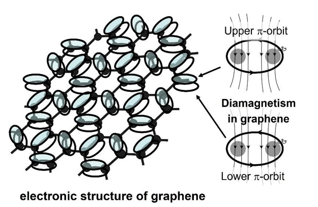
Figure 2: Graphene’s Electronic Structure Consists of Alternating Double and Single Bonds. The Unpaired Electrons in The Upper Andlower π-Orbits Create Orbital Magnetism.
The pattern has alternating double and single bonds. The covalent single σ-bond is the most important bonding in nature. It involves the sharing of two electrons between two adjacent atoms. But how to share?
An electron is a negatively charged particle and can be attracted by any positive electric field. When two atoms get closer and even closer, the higher energy valence electron (chemical name of unpaired electron) in one atom can also be attracted by the other nucleus, and vice versa. The maximum superimposed electric field of two identical nuclei forms a ring with radius a=0.7 L/2, L is the distance between the nuclei. Two unpaired electrons from two adjacent atoms enter the fixed ring with antiparallel spins, which cancel out the original orbital magnetism and lower the system energy.
The double bond is constructed by a covalent σ-bond and a conjugated π-bond. However, the various descriptions of the conjugated π-bond, such as the overlapping of two p-orbitals, the delocalization of a large π-bond, are still not possible to explain the fact that double bonds have color activity, electrical conductivity, chemical reactivity and ring aromaticity.
Figure 3 (a) is the newly proposed double bond. A conjugated π bond consists of two identical unpaired electrons with parallel spins. These two electrons are separated by the σ-bond. Each π-electron revolves around two nuclei and describes an elliptical orbit (named π-orbit). Figure 3 (b) appeared in the textbook of organic chemistry to explain the NMR result of a double bond. The newly proposed double bond is based on the NMR experimental fact. Unpaired electrons in the π-orbits create orbital magnetism, which is the key point for the special properties of a double bond.

Figure 3: (a). New Drawing of The Double Bond with Two Parallel Unpaired Electrons in Two π-Orbits. (b). Double Bond Structure in Organic Textbook.
The π-orbits in graphene are not fixed. Thermal vibrations of the C-C σ-bond cause stretching and contraction of the σ-bond. The π-orbits always revolve around two atoms at the shortest distance, which looks like delocalization of π-electrons.
This is exactly the same resonance structure as on the benzene ring. The ring mode of the infrared spectrum is about 1480 cm-1,corresponding to vibration frequency 1014 Hz. The Raman spectrum of graphene and graphite is about 1580 cm-1, , corresponding to vibration frequency 1014 Hz. The electron velocity is about 106 m/s. The π-electrons first revolve around the two atoms about many times before they meet a contraction motion of the σ-bond and change their position, making the single and double bonds to look like equalized.
In aromatic compounds, if one carbon atom is bonded to three carbon atoms, its resonance bond length is determined by X-rays to be 1.42 Å, such as crystallized C6(CH3)6 [15]. The same goes for graphene and graphite. If a carbon atom is bonded to two carbon atoms and one hydrogen atom, its resonant bond length is determined to be 1.40 Å by electron diffraction, as in the case of the gas single molecule C6H6 [16].
Graphene and graphite are diamagnetic. The magnetism is caused at atomic level by the orbital motion of unpaired electrons with magnetic momentum. The electron spin is always aligned along the external magnetic field. The orbit inside is diamagnetic (Fig 4a), outside is paramagnetic (Fig. 4b). The entire magnetism of a system is decided by the ratio of magnetic field line densities inside and outside the orbits, as shown in Figure 4 (a) and (b).

Figure 4: (a). Origin of Strong Diamagnetism Due to Contact of Electron Orbits. (b). The System Is Diamagnetic or Paramagnetic Depending on The Ratio of Magnetic Field Line Densities Inside and Outside the Orbits.
Due to the dense packing of the π-orbits, the graphene should be diamagnetic. This idea is consistent with the experimental evidence of the diamagnetism in graphene reported by Sepioni et al. in 2010 [2]. Many other special properties of graphene are just given by the unpaired electrons in the upper and lower π-orbits. For example, the opening of double bond for chemical addition reaction; under the force of an external electric field, the migrating of unpaired electrons in π-orbits in one direction to form an electric current; the electromagnetic layers above and under the honeycomb lattice leading to interaction with external electromagnetic waves (light); the strong anisotropic magnetoresistance, etc.
It must be clearly pointed out here that the electrons in the π-orbits are attracted by the electrostatic force of their atomic nuclei. The electrons themselves must move in the orbit at ultra-high speed, otherwise they will be attracted into the atomic nuclei. This speed is about 10+6 m/s, which means that an electron can make three revolutions around the Earth in one minute. It is not possible for electrons to form a cloud of probability, or to swim in crystal lattice.
The h-BN sheet is composed of equal amounts of boron and nitrogen atoms. The electron configuration of boron atom is 1s22s22p1. Three electrons in the outermost shell are hybridized to form three planar equal elliptical orbits. The electron configuration of nitrogen atom is 1s22s22p3. The three perpendicular atomic p-orbits with unpaired electrons can be transformed into three planar elliptical orbits under the influence of boron atoms. The two 2s2 electrons in the second shell remain in atomic orbit with antiparallel spins. The two-dimensional hexagonal network is constructed by covalent bonding between boron and nitrogen atoms, as shown in Figure 5.
Since there are no unpaired electrons in the system, h-BN sheet is insulating and chemically inert. The special lubrication function of h-BN should be attributed to the round 2s2 electron orbits on the nitrogen sites, which act as balloons to protect the sheets. Therefore, the h-BN material can be used as lubricant. The h-BN electronic structure in Figure 5 can be further supported by the fact that intrinsic h-BN is non-magnetic [17]. If 2s2 electrons are lone pairs (like in aromatic pyrrole), the entire h-BN should be paramagnetic. Any defects and doping can induce local magnetic states in the h-BN monolayer by dissociating 2s 2 electrons in atomic orbits, so the 2s2 electrons are metastable.

Figure 5: Electronic Structure of Hexagonal Boran Nitride (h-BN). There are no Unpaired electrons in the Molecule, making it Insulatingand Chemically Inert.
Without describing the electronic structure, h-BN sheet and graphene sheet are identical and both are electrically non-neutral. In the future, if we want to study two-dimensional sheet materials, we must consider the electronic structure.
Currently, when people study the electronic structure of graphene, they must use the most popular model: the “Dirac electronic structure of graphene”, which is based on density functional theory (DFT). Six Dirac-cones [18] are shown in Figure 6.

Figure 6: Dirac Electronic Structure of Graphene. This Structure Cannot Explain Graphene's Chemical, Electrical and Magnetic Properties
The indisputable fact that graphene and graphite have strong diamagnetic properties cannot be reflected in DFT at all. Therefore, this theory cannot explain the quantum Hall effect, superconductivity and anisotropic magnetoresistance exhibited by graphene. In fact, graphene is made up of just one type of carbon atom, which contains one type of unpaired electrons. If people always pursue complexity and ignore simplicity, it may make the problem more difficult to handle and understand.
New Explanation of Quantum Hall Effect in Graphene
Fixed gate voltage (Vg).
Figure 7 (a) is the quantum Hall effect in isolated single layer of graphene from graphite, discovered in 2005 by Zhang et al. at T=30
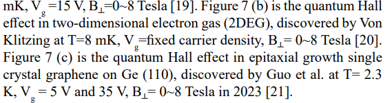

Figure 7: Quantum Hall Effect in Graphene and In Two-Dimensional Electron Gas. (a). Isolated Single Layer of Graphene from Graphite. (b). 2DEG at the Semiconductor Surface. (c). Epitaxial Growth Single Crystal Graphene on Ge (110).
Von Klitzing pointed out that a two-dimensional electron gas is absolutely necessary to observe the quantum Hall effect. It can be confirmed from Figure 7 that the quantum Hall effect of graphene and the quantum Hall effect of 2DEG are essentially the same. This suggests that the previously proposed electronic structure of graphene consisting of two layers of electron gas makes sense.
In the study of the quantum Hall effect in 2DEG, a very important concept is introduced, that is, electrons perform circular motion parallel to the surface under a vertical magnetic field, as shown in Figure 8.

Figure 8: Cyclotron Motion of Electrons in a 2D Electron Gas. The Electron Spin (Axis of Self-Rotation) is Perpendicular to The Orbit.
“Up to 1980 nobody expected that there exists an effect like the quantized Hall effect, which depends exclusively on fundamental constants and is not affected by irregularities in the semiconductor like impurities or interface effects” (Von Klitzing) [22]. In fact, 2DEG is a very pure system that is not affected by the nuclei. It is also the system that previous scientists tried to create to study the motion of pure electrons without the influence of the positively charged nuclei.
For example, Dehmelt used geonium atom [23] to study the cyclotron motion of a single electron under magnetic field of 5 Tesla.
“At present a microscopic theory that describes the QHE under real experimental conditions is not available (Von Klitzing) [22]”. The problem lies in the lack of correct understanding of ordinary conductivity and superconductivity. Electrons cannot swim in a crystal lattice like gas molecules in the air as described in many physics’ textbooks. They always perform orbital motion, and the unpaired electron orbits jump and move under the action of an external electric field to form a current, as shown in Figure 9 (a). If the spacing barrier between the orbits is too large to jumping over, it is Mott-insulator. If the orbits get in contact, it is superconductor without electrical resistance any more. However, under strong magnetic field, the electron orbits can be squeezed into smaller sizes.
The contact of the orbits is broken and superconductor turns into ordinary conductor, as shown in Figure 9 (b). The reduced orbits should be achieved by subtracting integer number of the circumference of the electron effective ball, because the electron ball rolls rather than slides in the orbit, which results in less energy change. This is the key to understand the superconducting phenomenon of intermittent zero resistance in the longitudinal current direction as the magnetic field strength increases, as shown in Figure 7 (b), diagram ρxx~B (T).
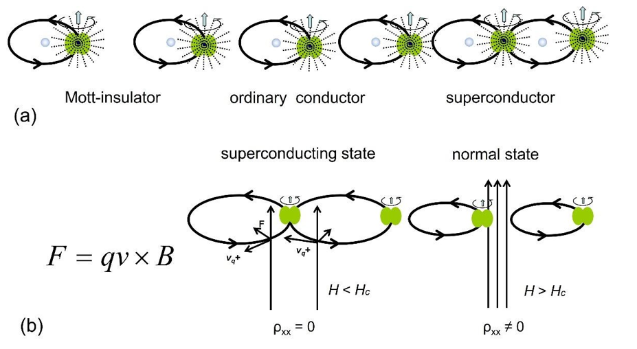
Figure 9: The Interspace Between Unpaired Electron Orbits Determines the Electrical Properties of a Substance. (a). Mott Insulator with Larger Interspace, Ordinary Conductor with Moderate Interspace, Superconductor with Zero Interspace. (b). Strong Magnetic Force Squeezes the Orbits into Smaller Sizes, Causing the Superconductor to Transform into An Ordinary Conductor.
In order to be able to explain the lateral movement of the charge carriers in the quantum Hall effect, we first need to understand the ordinary Hall effect at the atomic level. Hall discovered the Hall effect in a gold leaf in 1879 [24].
The experiment was carried out at room temperature, in perpendicular low magnetic field about 1 Tesla, with a small current of several hundred mA in longitudinal direction. A transverse Hall voltage was observed. Hall effect involves always three perpendicular directions: external electric field (E), external magnetic field (B) and lateral drifting of the charges, as shown in Figure 10 (a).

Figure 10: Ordinary Hall Effect. (a). Hall Experiment Setup. (b). Microscopic Mechanism of Hall effect.
What force drives electrons to drift laterally to produce the Hall voltage? The electron spins are oriented along the magnetic field lines, with the orbital plane (normal) parallel to the magnetic field. The trajectory of the movement of electrons (orbit) should be parallel to the sample surface. When an electron in the orbit is moving along or against the external electric field (E), the velocities of the electron on the left and right parts of the orbit are different. The net Lorentz force on the orbit is then not zero, as shown in Figure 10 (b). It is this force difference ΔF that drives the orbit to drift laterally.
Finally more electrons are accumulated on one edge, which establish a Hall voltage. Until the electrostatic repulsive force of the Hall voltage on the new coming electron and the magnetic driving force on the electron are balanced, the system is stable. Hall found that the B•I/VH = constant for a given metal. Therefore, Hall experiment can be used to characterize certain property of materials, such as densities of charge carriers.
Surface charge density n/S = B•I/VH•(1/e) = constant (certain metal)
Von Klitzing stated: “to observe a quantum Hall effect, a strong magnetic field perpendicular to 2DEG plane is necessary. The cyclotron orbit drifts in the direction perpendicular to the electric and magnetic field”. His statement is consistent with the new explanation of Hall effect in Figure 10 (a) and (b). Additionally, the quantum Hall effect shows much deeper information than the conventional Hall effect. The 2DEG is a pure system and has nothing to do with the characteristics of materials, so it can better reflect the nature of electrons under electric and magnetic fields. Von Klitzing found that the Hall resistances in the plateau’s states [Figure 7 (b), diagram ρxy~B (T)] are merely related to a constant over natural number 1, 2, 3.
RH=VH/I=Rk/i (i=1, 2, 3,…)
This constant is named after Klitzing RK.
Rk =h/e2
Here, h=6.62607040•10-34 J.S (Planck constant).
e=1.6021766208•10-19 C (unit charge).
h/e2=25812.807 Ω (theoretical value).
Rk=25812.80745 Ω (experimental value).
The value of the quantized Hall resistance at plateaus seems to be exactly correct for conductivity σxx =0 [20] (in the interior of the sample). The σxx is a function of the charge density. When it is zero it means either the charge density is zero or the electrons are localized and cannot flow. The plateau regime correspondences to superconducting behavior on one edge, as shown in Figure 11.

Figure 11: Quantum Hall Effect in 2D Electron Gas. Due to High Mobility of 2DEG, There Is No Charge Carries (σxx = 0) in the Bulk at The Plateaus State with Superconducting Edge.
The electron orbits are driven by transverse magnetic forces under a longitudinal electric field. More electron orbits are accumulated on one edge, even forming superconducting current. The main current (I) prefers to flow along the superconducting path, creating an insulating state inside due to the high mobility of 2DEG.
The supercurrent is formed by contact of the electron orbits; therefore, it is diamagnetic. In 2004, Von Klitzing, K. [25] observed that even if the QHE is characterized by a vanishing conductivity σxx (no current in the direction of the electric field), a finite current between source and drain of a Hall device can be established via this diamagnetic current. This phenomenon is supposed to be the so-called magnetic topological insulator occurring in a two- dimensional system. In this respect, the facts of his experiment are consistent with the theoretical explanation of this article.
Figures 12 (a) and (b) were presented by Von Klitzing in 2004 and 1986 respectively. He clearly pointed out the existence of diamagnetic currents in quantum Hall systems. However, the Hall voltage is measured by the charge carrier difference between the two transverse edges. Figure 12 (a) shows equal electron orbits on both edges, which is not a correct description for the quantum Hall effect. Figure 12 (b) is the result of his experiment. The voltage difference between the upper edge and the lower edge is U48, and the voltage difference from the center line to the lower edge is U46. The plateaus state in U48~B (T) diagram corresponds to superconducting current on upper edge, as mentioned in Figure 7 (b), and meanwhile, the U46 tends to zero. The experimental evidence from 1986 supports the theoretical idea of this paper (s. Fig.11). Therefore, the electrical conductivity in the bulk σxx =0, is due to the charge density being zero rather than the electrons being fixed and not flowing.

Figure 12: (a). Von Klintzing Diagram in 2004. (b). his Experimental Result in 1986. When U48 is at Plateaus State, U46 is Zero. The Experimental Result Supports the Proposal in Fig. 11.
Von Klitzing further discovered that the constant RK is also related to the reciprocal of the fine structure constant (α) [20].
α-1 =(h/e2) • (2/cε0 ) ≈ 137.035
Here, c speed of light, ε0 magnetic field constant.
The fine structure constant is derived from atomic emission spectra, which is related to the excited and ground states of the atoms caused by heating at 1600 C°. The quantum Hall phenomenon was observed at an ultra-low temperature near zero Kelvin. Why are they related?
The radius of the cyclotron orbit in 2DEG is inversely proportional to magnetic field strength. This is in line with the Bohr’s concept of electron orbits arranged in several shells in atoms. Atomic spectra are produced by the outward expansion of electron orbits caused by thermal energy, while the quantum Hall effect is produced by the inward contraction of electron orbits caused by squeezing force of strong magnetic fields. Whether inward or outward, the change in orbital size is quantized, as shown in Figure 13 (a) and (b).

Figure 13: The Correspondence Between the Integer Quantum Hall Effect and Bohr Shell Atomic Model.
How small can the orbit be compressed as the magnetic field increases? The repulsive force between two electrons in an orbit is Frepulsive = ke2/r2 (r is the diameter of the orbit). When the maximum value of the repulsive force is reached, the orbital diameter is minimum. This is most likely ν (i) = 1, corresponding to n = 1 in the Bohr shell atomic model. By analogy, ν=2 corresponds to n=2, and so on.
Another significant contribution to science made by the quantum Hall effect of two-dimensional electron gas is the revised understanding of the mechanism of superconductivity. For decades, it was thought that superconductivity was caused by Cooper pairs.
As the temperature decreases, the lattice shrinks, forcing two electrons to pair up. Two-dimensional electron gas has no crystal lattice at all, yet it exhibits superconductivity. The contact of unpaired electron orbits is the essence of superconductivity.
In short, the quantum Hall effect should involve the following factors:
o Electron circles ceaselessly.
o Hall effect.
o Superconductivity, accompanied by squeezing action.
o Bohr’s quantized electron orbit.
The external magnetic field has three functions here:
- Orienting the electron spin.
- Squeezing the electron orbit.
- Creating magnetic force difference to drive the orbit to drift laterally.
Once we understand the quantum Hall effect of two-dimensional electron gas, we can better understand the quantum Hall effect of graphene.
Du et al. described in 2009 that the evidence of collective behavior in graphene is lacking [26], in the mediate magnetic field range 0 to 12 Tesla, at 1 K to 80 K. Therefore, it is reasonable to believe that non-interacting electrons exist in graphene.
Each unpaired electron in graphene revolves around two carbon atoms. The upper and lower unpaired electrons are separated by the carbon network. As the magnetic field strength increases, the orbit becomes stepwise smaller. Under the influence of mutually perpendicular external electric fields and external magnetic fields, the unpaired electron orbits move to one edge, showing the quantum Hall effect that is exactly the same as that of 2DEG.
It must be pointed out here that the 2DEG is not affected by atomic nuclei, and the experimental results are quite clean. However, the two-dimensional electron gas in graphene is dragged by the positively charged carbon nuclei both laterally and longitudinally, so sharp peaks do not appear in the experimental curves (s. Fig. 7).
In 2007, Novoselov et al. reported “Room-temperature quantum Hall effect in graphene” [27]. The experiments were conducted in a single layer of graphene under fixed extremely strong magnetic fields of 29 Tesla and 45 Tesla respectively. In fact, this is no longer the quantum Hall effect in the true sense (Fig. 7). Under such strong magnetic fields, the electron orbits are already compressed to the minimum sizes, and the strong magnetic force drives the electrons to align neatly at the boundary. This quantized Hall effect is only related to the number of electrons and has nothing to do with orbital changes.
New Explanation of The Ambipolar Electric Field Effect of Single Layer Graphene
Graphene is found to exhibit a pronounced ambipolar electric field (Vg) effect in the absence of external magnetic field. Figure 14 is the experimental result from single layer graphene [28].

Figure 14: The Ambipolar Electric Field (Vg) Effect of Graphene in The Absence of External Magnetic Field. When n>0, The System Is Electron-Excess. When n<0, the System Is Electron-Deficient. This is Controlled by Gate Voltage.
The charge carriers (n) can be tuned continuously between electrons to holes in concentrations as high as 1013 cm–2 and their mobilities can exceed 10000 cm2/Vs by varying back gate voltage. This changes the longitudinal electric current (I) through graphene. This behavior is practically temperature independent [1,28,29].
Graphene is a zero-gap semiconductor or a conductor with resistivity of 10-6 Ω•cm. This is less than the resistivity of silver. Conduction of electricity is the movement of the negatively charged unpaired electrons in the longitudinal electric field resulting in a total movement of charges through the material. The movement of electrons can be realized by the drawing of positive electrode (drain) or by the pushing of negative electrode (source).
By applying a positive back gate voltage (Vg), more electrons are injected into the graphene sheet and are more likely to be located in the larger meshes of the graphene honeycomb lattice. Calculated according to crystal parameters, the larger mesh number (Fig. 2) is 1016 mesh•cm-2. This is higher than the highest concentration of 1013 cm–2 injected into graphene because repulsive forces between excess electrons limit the capacity. When the repulsive forces between the excess electrons increase the mobility of electrons toward the positive electrode, the conductivity (or current flow) increases and the resistivity decreases.
By applying a negative back gate voltage (Vg), more electrons are pulled out of graphene sheet and more positively charged C+ sites (holes) are exposed, which can attract negatively charged electrons, thereby allowing the electrons to easier flow through graphene sheet. This is the essence of the ambipolar electric field (Vg) effect.
The repulsive force of excess electrons and the attraction of electron-deficient holes (C+) both contribute to the flow of electrons.
Several concepts must be clarified here: A. The only things that can flow in graphene are unpaired electrons, while holes are C+ sites and they will not move. B. There is no two-dimensional gas with massless Dirac fermions in graphene [9]. Fermions refer to electrons. Already a hundred years ago, J. J. Thomson and R. A. Millikan had determined the charge and mass of the electron.
e = 1.602176634•10-19 C
me = 9.109383702•10-31 kg
Light Induced Superconductivity of Graphene at Ambient Conditions
Achieving superconducting behavior under normal temperature and pressure is the key to realizing the practical application of materials. In 2022, Tao et al. reported superconductivity of monolayer graphene stimulated by light at ambient conditions, as shown in Figure 15 [30].

Figure 15: Light-Induced Superconductivity of Single-Layer Graphene Under Ambient Conditions.
“Light” (electromagnetic waves) covers a very wide range, from radio wave to gamma-rays. To our previous knowledge, irradiation with light can result in the increase of the electrical conductivity in metals. After absorbing suitable light, the electron orbits are enlarged and the inter-spaces between the orbits are reduced. Once the orbits get in contact, superconductivity occurs, as shown in Figure 16.

Figure 16: Origin of The Light-Induced Superconductivity. After Absorbing Suitable Light, The Electron Orbits Are Enlarged and The Inter-Spaces Between the Orbits Are Reduced. Once the Orbits Get in Contact, Superconductivity Occurs.
This simple superconducting mechanism has been ignored by the current scientific and technological community. The orbits of unpaired electrons are either circular or elliptical. These orbits have electrical and magnetic properties and are the most active parts of the materials. When the electron orbits absorb thermal energy, light energy and kinetic energy, they shall expand. During falling back to ground state, the expanded orbits shrink to original sizes and emit light. This is the basic principle of atomic visible light spectrum and X-ray spectrum.
In 2016, Demsar et al. and Mitrano el al. reported possible light- induced superconductivity in K3C60 at high temperature [31,32]. In 2021, Budden et al. published evidence for metastable photo-induced superconductivity in K3C60 [33]. In 2023, Rowe et al. published resonant enhancement of photo-induced superconductivity in K3C60 [34]. Anyway, light-induced superconductivity continues to fascinate researchers.
As early as 1991, it was discovered that K3C60 is superconducting at ultra-low temperatures of several Kelvin. Pauling [35] wrote an article: “The structure of K3C60 and the mechanism of superconductivity”. He mentioned: “Analysis of the interatomic distances in the superconducting substance K3C60 indicates that each of the K atoms in tetrahedral interstices between C60 spheres accepts three electrons from C60, thus becoming quadricovalent; its four bonds resonate among the 24 adjacent carbon atoms to give a strong framework in which the negative charges are localized on these K atoms. The electric current is carried by the motion of positive charges (holes) through the network of C60 spheres and the K atoms in octahedral holes.
Superconductivity is favored by the localization of the negative charges on the tetrahedral K atoms and their noninvolvement in valence-bond resonance, decreasing the rate of mutual extinction of electrons and holes.” He is a very authoritative figure in the scientific community and won the 1954 Nobel Prize in Chemistry for determining the nature of the chemical bonds that connect atoms into molecules. However, this time his research on the mechanism of superconductivity failed. First, electric current is not carried by the motion of positive charges, which come from nuclei. Second, if the negative charges of electrons are localized, there will be no current realized. In 1993, Chen and Goddard III wrote: “Mechanism of superconductivity in K3C60” [36].
They tried to use Hamiltonian and Electron-Phonon Couplings to explain the superconductivity of K3C60. Whenever people introduce this first principle of Hamiltonian equation, they are immediately going to stuck into trouble right away. They complicate simple problems, and can no longer insight the essence of things. The Hamiltonian is included in the Schrödinger equation. The basis of the Schrödinger equation is the electron cloud probability assumption. Electrons do not appear randomly, and Schrödinger's hypothesis does not hold. The superconductivity of K3C60 can occur at ultralow or high temperatures, so the electron-phonon coupling is not the essence of superconductivity.
The C60 is a variation of single-layer graphene. We can use graphene’s electronic structure to explain K3C60 superconductivity. Figure 17 shows graphene-like C60 with alternative double and single bonds. The unpaired electrons in the π-orbits can come into contact with the unpaired electrons on the outermost surface of the potassium atom (acting as a bridges) by irradiation with light or by lowering temperature. This is the nature of K3C60 superconductivity.

Figure 17: Light-Induced Superconductivity in K3c60 At High Temperature. (a). The Crystal Structure of K3C60. (b). Explanation of the Phenomenon. C60 Belongs to The Graphene Family and Has the Same Alternating Single and Double Bond Electronic Structure. With the Help of The Outermost Single Electron of The Potassium Atom as A Bridge, the Supercurrent Is Conducted in C60.
Superconductivity in Ca-Intercalated Bilayer Graphene
Graphene deposited or intercalated with metallic atoms (Li, Na, K, Ru, Cs, Ca, Al, Yb etc.) exhibits superconducting behavior.
Ichinokura et al. [37] in 2016 reported the direct macroscopic measurements of the zero electrical resistance in Ca-intercalated bilayer graphene C6CaC6, which is regarded as the thinnest limit of Ca-intercalated graphite. They observed the superconducting behavior with the onset temperature (Tconset) of 4 K, as shown in Figure 18 (a) and (b). The ordering in the Ca layer is important for achieving superconductivity.

Figure 18: Superconductivity in Ca-intercalated bilayer (A-A-stack) graphene. (a). Schematic representation. (b). Experimental result.
Two single layers of graphene are arranged in an A-A stack. Ca atoms are arranged in a √3×√3R30° superstructure, as shown in Figure 19(a).

Figure 19: (a). Intercalated Pattern by Ca, Li, Cs, Rb. (b). The Presence of Unpaired Electrons in Graphene Limits Where Calcium Atoms Can Intercalate. The Ca Atoms Fall into the Larger Empty Space and Act as Bridges in Graphene, Much Like the Potassium Atoms Do in K3C60 Superconductors.
This pattern (Ca) has been confirmed with reflection-high-energy electron diffraction by Ichinokura et al. [37], Takahashi et al. (Li, Ca, Rb, Cs) [38], Huernpfner et al. (K) [39], and Margine et al. (Ca) [40]. According to the currently widely accepted hexagonal honeycomb structure of graphene, all meshes are equal. Why do metal atoms fit into specific meshes instead of randomly? So far, no research has addressed the configuration of unpaired electrons in graphene. However, these unpaired electrons do exist, otherwise graphene would be strongly electrically non-neutral. When the calcium atoms fall into the larger empty spaces, it is exactly the C6CaC6 √3 × √3R30° pattern, as shown in Figure 19 (b). Along the straight line formed by the calcium atoms, the π-orbits on the graphene are almost in contact with the 4s-orbits on the calcium atoms.
By cooling to a certain temperature, the orbits come into contact, and superconductivity occurs. The newly proposed electronic structure of graphene in this paper (Fig. 2) has been experimentally confirmed here. The electron-phonon coupling [40] is not responsible for the superconductivity in the intercalated graphene. The intercalated metal atoms have unpaired electrons in their outermost surfaces, which do not participate in chemical bonding in graphene but act as bridges, much like the potassium atoms do in K3C60 superconductors.
Ichinokura found that when a perpendicular external magnetic field is applied to the surface of C6CaC6 graphene, the superconductivity disappears, and when the temperature is increased, the superconductivity disappears [37]. They are two typical characteristics of superconductors. Magnetic force can squeeze the electron orbits into smaller sizes. The contact of the orbits is destroyed, superconductor turns into normal conductor (s. Fig. 9b). As the temperature increases, the thermal vibration amplitude of atoms increases, causing the distance between atoms to become larger and the corresponding orbital gap to become larger. If the orbital contact is broken, the superconductor becomes a regular conductor.
Many phenomena can be explained by understanding the superconducting mechanism of C2CaC2. As long as the outermost unpaired electrons of the metal atoms come into contact with the unpaired electrons in graphene, a superconductor can be formed. Examples include superconductivity in lithium-decorated single- layer graphene [41], and superconductivity in Ca-intercalated on top of bilayer, between the bilayer or even beneath the bilayer graphene [42,43]. The superconducting behavior of C6Cs2C6 can also be explained by C6CaC6. Two layers of Cs atoms serve the upper and lower layers of graphene respectively [44]. As Ichinokura pointed out that “The number of graphene layers in this multilayer graphene is not necessarily clear for the occurrence of superconductivity” [37]. The most important thing is how to form the contact of unpaired electron orbits.
The superconducting phenomenon caused by intercalation will not only appear in graphene, but also in layered kagome materials. For example, K, Rb, and Cs intercalated V3Sb5 kagome sheets show superconducting phenomena (Cs Tc=2.5K, K Tc =0.9K) [45, 46]. Figure 20 is the structure of V3Sb5 slab and the electronic structure of Sb2 atoms.
Fig. 20. (a). Crystal structure of kagome V3Sb5. (b). Electronic structure of Sb (2) upper and lower the sheet.

Figure 20: (a). Crystal Structure of kagome V3Sb5. (b). Electronic Structure of Sb (2) Upper and Lower The Sheet.
The 5s25p3 electrons at the Sb (2) site undergo sp3 hybridization. The three unpaired electrons of the Sb atom are connected to the three vanadium atoms, leaving two unpaired electrons as lone pairs.
The lone pair of electrons has the same property as π-electrons, which have orbital magnetism and can move in external electric field. Figure 21 (a) is the crystal structure of KV3Sb5 [46]. Figure 21 (b) highlights the nearest unpaired electrons in the system, which are responsible for superconductivity. Once the orbits come into contact by lowering the temperature, these quasi-two-dimensional kagome materials become superconducting.

Figure 21: KV3Sb5 Superconductor. (a). Crystal Structure. (b) The Nearest Unpaired Electrons In The System. The Outermost Single Electron Of K-Atom Acts as Bridge to Reduce the Interspace Distance of The Unpaired Electrons (include lone pair) in the System, To Facilitate Orbital Contact.
So far, a great deal of work has been done to theoretically explain the superconductivity of kagome [47]. This new understanding will help people get out of the confusion.
Superconductivity in Twisted Bilayer and Trilayer Graphene
In 2018, Cao et al. reported for the first time the gate-voltage tunable superconductivity of twisted bilayer graphene with a magic angle of about 1.1° at a critical temperature (Tc) of 1.7 K, as shown in Figure 22 (a) [48]. Since then, a lot of researches have been done in this field. In 2021, Park et al. reported that a gate- tunable ultra-strong coupling superconductivity of about Tc=2 K was achieved in a new magic-angle system, consisting of three adjacent graphene layers sequentially twisted by θ and –θ (~1.6°), as shown in Figure 22 (b) [49].

Figure 22: Superconductivity in Twisted Bilayer (a) and Trilayer (b) Graphene. The Moiré Superlattices Are Not the Cause of Superconductivity.
It is said that the Moiré superlattices have recently emerged as a novel platform where correlated physics and superconductivity can be studied with unprecedented tunability. This is a wrong research direction. If the h-BN sheets are twisted in the same way as the twisted graphene, the Moiré pattern is exactly the same, but there will be no superconducting behavior. Recent research (July, 2024) [50] shows that the superconducting mechanism of twisted graphene still focuses on the Moiré pattern, electron- phonon coupling, and charge fluctuation. The unconventional superconductivity of the overlapping layers is not caused by these factors. In particular, the superconducting transition temperature approaches absolute zero, the amplitude of thermal vibrations approaches zero, and there are no charge fluctuations or phonon- mediated electron interactions.
The superconductivity of twisted graphene is caused by the unpaired π-electrons in the interfaces. Twist and mismatch operations can lead to stable contact of unpaired electron orbits and robust superconductivity.

Figure 23: (a). The Lower Unpaired Electron Orbits Decomposed from the First Graphene Sheet. (b). The Upper Unpaired Electron Orbits Decomposed from the Second Graphene Sheet After Being Twisted by 1.1°.
Figure 23 (a) shows the lower unpaired electron orbits decomposed from the top graphene sheet, and Figure 23 (b) shows the upper unpaired electron orbits decomposed from the bottom graphene sheet after being twisted by 1.1°. Superimposing these two drawings with a lateral mismatch of about 1Å, it can be seen that every two rows of the electron orbits are almost in contact, as shown in Figure 24 (a). The gate-voltage applied on the topmost and bottommost surfaces of the twisted bilayer will force the unpaired electron orbits in the interface to make contact, resulting in the superconducting state, as shown in Figure 24 (b).
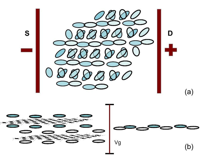
Figure 24: (a). Top View of Unpaired Electron Orbits in The Interface of The Twist Bilayer Graphene. (b). Side View of The Twist Bilayer Graphene. Before Gate Voltage It Is an Insulator and After Gate Voltage It Is A Superconductor.
In 2021, Tom Garlinghouse of Princeton University reported: “The superconductivity of Magic Graphene and that of High-Temperature (cuprate) superconductors have uncanny Resemblance” [51]. But unfortunately, they didn't come to any convincing conclusions about the relationship between the two superconductors. Indeed, graphene superconductor is similar to cuprate high-temperature superconductor, because both conduct supercurrent in layers through elliptical unpaired electron orbits, as shown in Figure 25.

Figure 25: Cuprate Superconductor. This Ceramic Compound Is an Insulator at Room Temperature and A Superconductor below 93 K. Superconducting Behavior Is Similar to Twisted Graphene.
The emergence of high-temperature superconductivity is another challenge to Bardeen-Cooper-Schrieffer (BCS) Cooper pair theory [52]. This Boson-like quantum state occurs only at sufficient low temperature near zero Kelvin. In Garlinghouse’s article, he mentioned that “his colleague Oh published paper “Evidence for unconventional superconductivity in twisted bilayer graphene” in 2021 [53]. They provided a preponderance of evidence for a non-BCS mechanism for superconductivity in magic angle twist bilayer graphene”. On this they are right. Cooper pairs do not exist in nature. BCS theory cannot explain the strong diamagnetism of superconductors. Oh et al. observed the experimental signatures for unconventional superconductivity of twisted bilayer graphene using scanning tunneling microscope (STM).
In 2022, Kim et al. published the paper “Evidence for unconventional superconductivity in twisted trilayer graphene”, also using STM [54]. The principle of STM is the tunneling of unpaired electrons from sample surface to metallic tip by perpendicular bias voltage. Therefore, it is difficult to find the motion of π-electrons in graphene parallel to the surface. Oh et al. believed that the superconductivity of twisted bilayer graphene resembles a nodal superconductor and provides experimental evidence with an anisotropic pairing mechanism. This statement is far from reality.
In 2021, Cao et al. reported that the magic-angle twisted trilayer graphene exhibits superconductivity up to in-plane magnetic fields in excess of 10 T [55]. According to Cao's schematic of the experimental system, their magnetic field is along Vxx direction. In the same year, Qin & MacDonald reported: “In-plane critical magnetic field in magic-angle twisted trilayer graphene”. They pointed out that superconductivity in magic-angle twisted trilayer graphene survives to in-plane magnetic fields much stronger than to the in-plane magnetic field in twisted bilayer graphene [56].
Superconductors have two special features: diamagnetism (Meissner levitating effect), and magnetic field destruction of superconductivity, as shown in Figure 9 (b). Why can twisted trilayer graphene survive such a strong magnetic field without destroying superconductivity? The key is that the applied magnetic field lies within the plane of the graphene and parallel to the orbits. The electron spin (tiny magnet) aligns always along the external magnetic field line, and the orbit is perpendicular to the electron spin. However, due to the constraints between layers, the orbits are not upright and remain within the plane of the magnetic field. In this way, the magnetic field cannot exert a magnetic force on the orbit, and it is impossible to squeeze the orbit. Contact between the orbits is then maintained and the superconducting state is not destroyed. This also explains why the trilayer is more likely to survive the destruction of the magnetic field than the bilayer, as shown in Figure 26.

Figure 26: Superconductivity of Twisted Trilayer Graphene Survives High In-Plane Magnetic Fields in Excess of 10 T. There is Almost No Magnetic Squeezing force on the Orbit When Magnetic Field Is In-Plane.
At present, there is still a lot of research works that believed that the twisted Moiré superlattice structure is responsible for the superconducting behavior of multilayer graphene. In fact, superconductivity of few-layer graphene can occur without twisting, and has nothing to do with Moiré superlattices.
In 2022, Heikkilä reported in science “Surprising superconductivity of graphene: An ordinary graphene bilayer exhibits extraordinary superconductivity”, as shown in Figure 27 [57]. In the presence of a large perpendicular electric field (displacement field), Bernal- stacked (A-B) bilayer graphene (BLG) shows metallic phases. When applying in plane magnetic field (165 mT), the bilayer graphene exhibits superconductivity [58].

Figure 27: Without Twisted, An Ordinary Bilayer Graphene (A-B Stack) Shows Superconductivity in The Presence of a Large Perpendicular Electric Field and Applying In-Plane Magnetic Field.
An electron is a self-rotating negatively charged particle. It can be attracted by any positive electric field. Under the superimposed electric field of the large electric displacement field (E) and the positive electric field of carbon atoms, the trajectory of electrons will change from the original elliptical π-orbits around two carbon atoms to an ellipsoid of lone pair of electrons revolving one carbon atom. It is precisely the A-B stack of graphene that provides the space for these ellipsoids to move. After applying external in plane magnetic field (B), the electron spins align along the external magnetic field line.
The ellipsoid changes to elliptical orbits. Electric field E, magnetic field B and Lorentz force difference on the orbits form three perpendicular directions, then the electron orbits are drove to one edge of the sample, Hall voltage is developed. When enough electrons accumulate at one edge and an electric current is applied, a superconducting band appears. Macroscopically, metallic graphene changes to superconductor. The in-plane magnetic field strength applied to A-B bilayer graphene is about 165 mT (0.1 T), which is quite weak compared to in-plane magnetic field of 10 T applied to twisted trilayer graphene. By understanding the configuration of the electron orbits, we can gain insights of the superconductivity of few-layer graphene.
All current graphene structural diagrams lack electronic motion states, which are the soul of the material's active properties. We can "see" atoms directly, but not the surrounding electrons. There is an urgent need to cross the threshold to study the motion state of electrons in materials. I have made some descriptions of the various motions of electrons in graphene, hoping to partially fill the scientific gaps
Conclusions
Graphene consists of only two things: the stable hexagonal honeycomb infinite network combined by covalently bonded carbon atoms, and the active unpaired Ï?-electrons. Graphene serves as a platform that allows us to study a lot of fundamental concepts of electron motion. For example: electron spin, orbital magnetism, covalent bond, double bond, lone pair of electrons, mechanism of electrical conductivity and superconductivity, quantum Hall effect at atomic level.Acknowledgements
The author would like to thank Dr. Thomas VON LARCHER, Senior Editor, Research Publishing, Springer Nature, for his many suggestions in revising this article.
Funding
Not Applicable.Clinical Trial Number
not applicable.
Ethics, Consent to Participate, and Consent to Publish declarations: not applicable.
References
- Novoselov, K. S., Geim, A. K., Morozov, S. V., Jiang, D.E., Zhang, Y., Dubonos, S. V., ... & Firsov, A. A. (2004). Electric field effect in atomically thin carbon films. Science, 306(5696), 666-669.
- Sepioni, M., Nair, R. R., Rablen, S., Narayanan, J., Tuna, F., Winpenny, R., ... & Grigorieva, I. V. (2010). Limits on intrinsic magnetism in graphene. Physical Review Letters, 105(20), 207205.
- Ganguli, N., & Krishnan, K. S. (1941). Magnetic and other properties of the free electrons in graphite. Proceedings of the Royal Society of London. Series A. Mathematical and Physical Sciences, 177(969), 168-182.
- Geim, A. K., & Novoselov, K. S. (2007). The rise of graphene.Nature materials, 6(3), 183-191.
- Xin, N., Lourembam, J., Kumaravadivel, P., Kazantsev, A. E., Wu, Z., Mullan, C., ... & Berdyugin, A. I. (2023). Giant magnetoresistance of Dirac plasma in high-mobility graphene. Nature, 616(7956), 270-274.
- Gautam, R., Marriwala, N., & Devi, R. (2023). A review: Study of Mxene and graphene together. Measurement: Sensors, 25, 100592.
- Nature editorial. 15 years of graphene electronics. Work on two-dimensional materials continues to yield both surprises and new devices. Nature Electronics 2, 369 (2019).
- Worku, A. K., & Ayele, D. W. (2023). Recent advances of graphene-based materials for emerging technologies. Results in Chemistry, 5, 100971.
- Novoselov, K. S., Geim, A. K., Morozov, S. V., Jiang, D.,Katsnelson, M. I., Grigorieva, I. V., ... & Firsov, A. A. (2005). Two-dimensional gas of massless Dirac fermions in graphene. Nature, 438(7065), 197-200.
- Urade, A. R., Lahiri, I., & Suresh, K. S. (2023). Graphene properties, synthesis and applications: a review. Jom, 75(3), 614-630.
- Jain, P., Rajput, R. S., Kumar, S., Sharma, A., Jain, A., Bora, B. J., ... & Bhowmik, A. (2024). Recent advances in graphene-enabled materials for photovoltaic applications: a comprehensive review. ACS omega, 9(11), 12403-12425.
- Sang, M., Shin, J., Kim, K., & Yu, K. J. (2019). Electronic and thermal properties of graphene and recent advances in graphene based electronics applications. Nanomaterials, 9(3), 374.
- Zan, X., Guo, X., Deng, A., Huang, Z., Liu, L., Wu, F., ... &Zhang, G. (2024). Electron/infrared-phonon coupling in ABC trilayer graphene. Nature Communications, 15(1), 1888.
- Ares, P., & Novoselov, K. S. (2022). Recent advances in graphene and other 2D materials. Nano Materials Science, 4(1), 3-9.
- Lonsdale, K. (1929). The structure of the benzene ring in C6 (CH3)6. Proceedings of the Royal Society of London. Series A, Containing Papers of a Mathematical and Physical Character, 123(792), 494-515.
- Mark, H., & Wierl, R. (1930). Neuere ergebnisse derelektronenbeugung. Naturwissenschaften, 18(36), 778-786.
- Sharma, R. & Kumar, A. (2024). Chapter 5 - Magnetic, mechanical, and tribological properties of hexagonal boron nitride. Hexagonal Boron Nitride 125-157 (1st ed.). Elsevier.
- Castro Neto, A. H., Guinea, F., Peres, N. M., Novoselov, K. S., & Geim, A. K. (2009). The electronic properties of graphene. Reviews of Modern Physics, 81(1), 109-162.
- Zhang, Y., Tan, Y. W., Stormer, H. L., & Kim, P. (2005). Experimental observation of the quantum Hall effect and Berry's phase in graphene. Nature, 438(7065), 201-204.
- Von Klintzing, K. (1986). The quantum Hall effect. Reviews ofModern Physics. 58(3), 519-531.
- Guo, W., Zhang, M., Xue, Z., Chu, P. K., Mei, Y., Tian, Z., & Di, Z. (2023). Extremely High Intrinsic Carrier Mobility and Quantum Hall Effect of Single Crystalline Graphene Grown on Ge (110). Advanced Materials Interfaces, 10(23), 2300482.
- Von Klitzing, K. Dorda, G., & Pepper, M. (1980). New method for high-accuracy determination of the fine-structure constant based on quantized Hall resistance. Physical Review Letters, 45(6), 494.
- Dehmelt, H. G. (1989). Experiments with an Isolated Subatomic Particle at Rest. Nobel Lecture in Physics. 583- 595.
- Hall, E. H. (1879). On a new action of the magnet on electriccurrents. American Journal of Mathematics, 2(3), 287-292.
- Von Klitzing, K. (2004). 25 Years of Quantum Hall Effect (QHE) A Personal View on the Discovery, Physics and Applications of this Quantum Effect. Séminaire Poincaré 2. 1-16.
- Du, X., Skachko, I., Duerr, F., Luican, A., & Andrei, E. Y. (2009). Fractional quantum Hall effect and insulating phase of Dirac electrons in graphene. Nature, 462(7270), 192-195.
- Novoselov, K. S., Jiang, Z., Zhang, Y., Morozov, S. V., Stormer,H. L., Zeitler, U., ... & Geim, A. K. (2007). Room-temperature quantum Hall effect in graphene. Science, 315(5817), 1379- 1379.
- Kretinin, A. V., Cao, Y., Tu, J. S., Yu, G. L., Jalil, R., Novoselov,K. S., ... & Gorbachev, R. V. (2014). Electronic properties of graphene encapsulated with different two-dimensional atomic crystals. Nano Letters, 14(6), 3270-3276.
- Novoselov, K. S., Morozov, S. V., Mohinddin, T. M. G., Ponomarenko, L. A., Elias, D. C., Yang, R., ... & Geim, A.K. (2007). Electronic properties of graphene. Physica Status Solidi (b), 244(11), 4106-4111.
- Tao, C. K., Tao R., Kang, T. Y., Hu, M. Y., Wu, Y. J., Yang,M. K., …& Zhang, Y. J. (2022). Graphene Superconductivity at Roomâ?Temperature of a Wide Range and Standard Atmosphere, Based on Vacuum Channels and Whiteâ?Light Interferometry. Advanced Electronic Materials, 8(1), 2100595.
- Demsar, J. (2016). Light-induced superconductivity. Nature Physics, 12(3), 202-203.
- Mitrano, M., Cantaluppi, A., Nicoletti, D., Kaiser, S., Perucchi, A., Lupi, S., ... & Cavalleri, A. (2016). Possible light-induced superconductivity in K3C60 at high temperature.Nature, 530(7591), 461-464.
- Budden, M., Gebert, T., Buzzi, M., Jotzu, G., Wang, E., Matsuyama, T., ... & Cavalleri, A. (2021). Evidence for metastable photo-induced superconductivity in K3C60. Nature Physics, 17(5), 611-618.
- Rowe, E., Yuan, B., Buzzi, M., Jotzu, G., Zhu, Y., Fechner, M., ... & Cavalleri, A. (2023). Resonant enhancement of photo-induced superconductivity in K3C60. Nature Physics, 19(12), 1821-1826.
- Pauling, L. (1991). The structure of K3C60 and the mechanism of superconductivity. Proceedings of the National Academy of Sciences, 88(20), 9208-9209.
- Chen, G., & Goddard 3rd, W. A. (1993). Mechanism of superconductivity in K3C60. Proceedings of the National Academy of Sciences, 90(4), 1350-1353.
- Ichinokura, S., Sugawara, K., Takayama, A., Takahashi, T., & Hasegawa, S. (2016). Superconducting calcium-intercalated bilayer graphene. ACS nano, 10(2), 2761-2765.
- Takakashi, T., Sugawara, K., Ichinokura, S., Takayama, A., & Hasegawa, S. (2017). Two-Dimensional Superconductivity in Intercalated Bilayer Graphene. Hyomen Kagaku, 38(9), 460- 465.
- Huempfner, T., Otto, F., Forker, R., Müller, P., & Fritz, T. (2023). Superconductivity of Kâ?intercalated epitaxial bilayer graphene. Advanced Materials Interfaces, 10(11), 2300014.
- Margine, E. R., Lambert, H., & Giustino, F. (2016). Electron- phonon interaction and pairing mechanism in superconducting Ca-intercalated bilayer graphene. Scientific Reports, 6(1), 21414.
- Ludbrook, B. M., Levy, G., Nigge, P., Zonno, M., Schneider, M., Dvorak, D. J., ... & Damascelli, A. (2015). Evidence for superconductivity in Li-decorated monolayer graphene. Proceedings of the National Academy of Sciences, 112(38), 11795-11799.
- Endo, Y., Fukaya, Y., Mochizuki, I., Takayama, A., Hyodo, T., & Hasegawa, S. (2020). Structure of superconducting Ca-intercalated bilayer Graphene/SiC studied using total- reflection high-energy positron diffraction. Carbon, 157, 857- 862.
- Toyama, H., Akiyama, R., Ichinokura, S., Hashizume, M., Iimori, T., Endo, Y., ... & Hasegawa, S. (2022). Two- dimensional superconductivity of Ca-intercalated graphene on SiC: vital role of the interface between monolayer graphene and the substrate. ACS nano, 16(3), 3582-3592.
- Lin, Y. C., Matsumoto, R., Liu, Q., Solís-Fernández, P., Siao,M. D., Chiu, P. W., ... & Suenaga, K. (2024). Alkali metal bilayer intercalation in graphene. Nature Communications, 15(1), 425.
- Ortiz, B. R., Teicher, S. M., Hu, Y., Zuo, J. L., Sarte, P. M., Schueller, E. C., ... & Wilson, S. D. (2020). CsV3Sb5: a Z2 topological with a superconducting ground state. PhysicalReview Letters, 125(24), 247002.
- Cao, Y., Fatemi, V., Fang, S., Watanabe, K., Taniguchi, T., Kaxiras, E., & Jarillo-Herrero, P. (2018). Unconventional superconductivity in magic-angle graphene superlattices.Nature, 556(7699), 43-50.
- Jiang, K., Wu, T., Yin, J. X., Wang, Z., Hasan, M. Z., Wilson,S. D., ... & Hu, J. (2023). Kagome superconductors AV3Sb5 (A= K, Rb, Cs). National Science Review, 10(2), nwac199.
- Cao, Y., Fatemi, V., Fang, S., Watanabe, K., Taniguchi, T., Kaxiras, E., & Jarillo-Herrero, P. (2018). Magic-angle graphene superlattices: a new platform for unconventional superconductivity. arXiv preprint arXiv:1803.02342.
- Park, J. M., Cao, Y., Watanabe, K., Taniguchi, T., & Jarillo- Herrero, P. (2021). Tunable strongly coupled superconductivity in magic-angle twisted trilayer graphene. Nature, 590(7845), 249-255.
- Long, M., Jimeno-Pozo, A., Sainz-Cruz, H., Pantaleón, P. A., & Guinea, F. (2024). Evolution of superconductivity in twisted graphene multilayers. Proceedings of the National Academy of Sciences, 121(32), e2405259121.
- Tom Garlinghouse for the Department of Physics, PrincetonUniversity, Oct. 20. 2021.
- Bardeen, J., Cooper, L. N., & Schrieffer, J. (1957). Theory ofsuperconductivity. Phys. Rev, 108, 1175.
- Oh, M., Nuckolls, K. P., Wong, D., Lee, R. L., Liu, X., Watanabe, K., ... & Yazdani, A. (2021). Evidence for unconventional superconductivity in twisted bilayer graphene. Nature, 600(7888), 240-245.
- Kim, H., Choi, Y., Lewandowski, C., Thomson, A., Zhang, Y., Polski, R., ... & Nadj-Perge, S. (2022). Evidence for unconventional superconductivity in twisted trilayer graphene. Nature, 606(7914), 494-500.
- Cao, Y., Park, J. M., Watanabe, K., Taniguchi, T., & Jarillo- Herrero, P. (2021). Pauli-limit violation and re-entrant superconductivity in moiré graphene. Nature, 595(7868), 526-531.
- Qin, W., & MacDonald, A. H. (2021). In-plane critical magnetic fields in magic-angle twisted trilayer graphene. Physical Review Letters, 127(9), 097001.
- Heikkilä, T. T. (2022). Surprising superconductivity of graphene. Science, 375(6582), 719-720.
- Zhou, H., Holleis, L., Saito, Y., Cohen, L., Huynh, W., Patterson, C. L., Yang, F., Taniguchi, T., Watanabe, K., & Young, A. F. (2022). Isospin magnetism and spin-polarized superconductivity in Bernal bilayer graphene. Science, 375(6582), 774-778.