
Annals of Civil Engineering and Management(ACEM)
ISSN: 3065-9779 | DOI: 10.33140/ACEM


Research Article - (2025) Volume 2, Issue 2
Advanced Nanostructured Materials for Civil Engineering Applications: Enhancing Infrastructure Durability through ZnO-Based Protective Systems
Received Date: May 06, 2025 / Accepted Date: Jun 05, 2025 / Published Date: Jun 09, 2025
Copyright: ©Â©2025 Arash Vaghef-Koodehi. This is an open-access article distributed under the terms of the Creative Commons Attribution License, which permits unrestricted use, distribution, and reproduction in any medium, provided the original author and source are credited.
Citation: Vaghef-Koodehi, A. (2025). Advanced Nanostructured Materials for Civil Engineering Applications: Enhancing Infrastructure Durability through ZnO-Based Protective Systems. Ann Civ Eng Manag, 2(2), 01-10.
Abstract
Infrastructure protection against electrical surges and environmental hazards remains a critical challenge in modern civil engineering. This study develops and characterizes advanced nanostructured ZnO-based protective systems specifically designed for civil engineering applications. We employed Spark Plasma Sintering (SPS) to fabricate multi-component ZnO protective materials, demonstrating superior performance compared to conventional processing methods. These materials exhibit exceptional electrical properties, including high nonlinearity coefficients (α > 50), minimal leakage currents (<5 μA/cm2), and remarkable energy absorption capabilities (>370 J/cm3), making them ideal for protecting civil infrastructure against electrical surges and lightning strikes. Microstructural characterization revealed that SPS-processed materials feature uniform nanostructures with controlled grain sizes (0.3-1.2 μm) and optimized grain boundary characteristics. High-resolution electron microscopy confirmed thinner, more uniform bismuth-rich grain boundary layers (3-8 nm) in SPS samples compared to conventional specimens (10-25 nm). The established processing- structure-property relationships provide civil engineers with a robust framework for implementing next-generation protective systems in critical infrastructure, including bridges, high-rise buildings, and power distribution networks. Our findings demonstrate that precise nanoscale engineering enables the development of protective materials with exceptional performance metrics that significantly exceed current industry standards, potentially extending infrastructure service life and reducing maintenance costs.
Keywords
Nanostructured Protective Materials, Civil Infrastructure Protection, Spark Plasma Sintering, Electrical Surge Protection, Advanced Construction Materials, Infrastructure Durability Enhancement
Key Findings: SPS-processed materials achieved exceptional electrical properties including high nonlinearity coefficients (α > 50), minimal leakage currents (<5 μA/cm²), and remarkable energy absorption capabilities (>370 J/cm³). Microstructural analysis revealed controlled grain sizes (0.3-1.2 μm) with optimized bismuth-rich grain boundary layers (3-8 nm thickness).
Novel Contributions: This work establishes quantitative processing-structure-property relationships through systematic parameter optimization. We demonstrate a 100% improvement in nonlinearity coefficient and energy absorption capacity compared to conventional methods. The developed materials maintain over 95% performance after accelerated aging equivalent to 10 years, significantly exceeding current industry standards.
Practical Impact: These findings provide civil engineers with scientifically-validated guidelines for implementing next-generation protective systems in critical infrastructure including bridges, high-rise buildings, and power distribution networks, potentially extending service life while reducing maintenance costs
Introduction
Current Challenges in Infrastructure Protection
Modern civil infrastructure faces unprecedented challenges from increasingly severe environmental conditions and power surges in highly electrified systems [1]. Traditional protective approaches suffer from several critical limitations:
1. Separate system installations requiring complex integration,
2. Inconsistent performance under varying conditions, and
3. High maintenance costs throughout service life [2,3].
Recent infrastructure failures highlight these vulnerabilities. Lightning strikes cause millions of dollars in damage annually to bridges and high-rise buildings [4]. Power surge incidents in electrical distribution networks result in costly equipment failures and service interruptions [5]. These challenges necessitate innovative protective solutions that can be seamlessly integrated into infrastructure design.
Knowledge Gap and Research Significance
While previous studies have explored ceramic materials for specialized applications, three critical gaps remain unaddressed:
• Limited Civil Engineering Focus: Most research targets electronic applications rather than infrastructure protection.
• Insufficient Processing Optimization: Systematic processing-property relationships remain unexplored.
• Lack of Durability Validation: Long-term performance under realistic infrastructure conditions is poorly understood [6,7].
Unlike previous studies that focus on individual material properties, this research establishes comprehensive processing-structure-property relationships specifically for civil engineering applications. We demonstrate how advanced processing techniques can simultaneously optimize multiple protective properties while ensuring long-term durability.
Research Objectives and Approach
This study addresses the knowledge gaps through four specific objectives:
• Develop multi-component ZnO protective materials using advanced Spark Plasma Sintering.
• Establish quantitative relationships between processing parameters and protective properties Validate long-term performance under simulated infrastructure conditions.
• Provide practical guidelines for implementation in civil engineering applications
Methodological Innovation
We combine systematic processing optimization with comprehen- sive microstructural characterization and performance validation, providing a complete framework for engineering protective mate- rials with tailored properties.
Experimental Methodology
Material Formulation and Preparation
The multi-component protective material system was formulated based on systematic optimization using the Taguchi method [8]. The composition (mol%) was: 97.0 ZnO, 0.5 0.5 Biâ??Oâ??, 0.5 Sbâ??Oâ??, 0.5 Coâ??Oâ??, 0.3 MnOâ??, 0.3 Crâ??Oâ??, 0.3 NiO, 0.2 SiOâ??, 0.2 SnOâ??, and 0.2 Alâ??Oâ??. Raw materials with optimized particle sizes were employed as detailed in Table 1.
|
Material |
Particle Size (nm) |
Purity (%) |
Source |
Reference |
|
ZnO |
70-100 |
99.9 |
Sigma-Aldrich, USA |
[9] |
| Biâ??Oâ?? |
30-50 |
99.8 |
Merck, Germany |
[10] |
| Sbâ??Oâ?? |
40-60 |
99.9 |
Alfa Aesar, USA |
[11] |
| Coâ??Oâ?? |
20-40 |
99.7 |
Sigma-Aldrich, USA |
[9] |
| MnOâ?? |
30-50 |
99.8 |
Merck, Germany |
[10] |
| Crâ??Oâ?? |
40-60 |
99.9 |
Alfa Aesar, USA |
[12] |
|
NiO |
30-50 |
99.8 |
Sigma-Aldrich, USA |
[13] |
| SiOâ?? |
15-30 |
99.9 |
Evonik, Germany |
[14] |
| SnOâ?? |
20-40 |
99.9 |
Merck, Germany |
[10] |
| Alâ??Oâ?? |
15-25 |
99.95 |
Sumitomo, Japan |
[15] |
Table 1: Raw Materials Specifications for the Multi-Component ZnO Protective System
Formulation Rationale
ZnO serves as the primary nonlinear element, while Biâ??Oâ?? form intergranular phases that control electrical barriers. Transition metal oxides fine-tune barrier characteristics, and ceramic additives enhance mechanical stability under infrastructure loading conditions.
The powders were homogenized using a two-step approach specifically designed to maintain nanoparticle integrity while ensuring uniform distribution of all components:
• Dry mixing in a planetary ball mill for 2 hours at 250 rpm.
• Wet milling in ethanol medium for 5 hours with zirconia balls (ball-to-powder ratio 10:1).
Processing Techniques
Two distinct processing approaches were employed to investigate the influence of sintering techniques on nanostructural development and resulting protective properties:
Conventional Sintering (CS):
• Uniaxial pressing at 200 MPa to form 20 mm diameter discs.
• Conventional sintering in a programmable furnace at temperatures ranging from 1000°C to 1200°C.
• Heating rate: 5°C/min.
• Holding time: 2-5 hours.
• Natural cooling in the furnace.
Spark Plasma Sintering Conditions:
• Temperature range: 800-900°C (optimized at 850°C).
• Holding time: 5-15 minutes (optimized at 10 minutes).
• Applied pressure: 30-60 MPa (optimized at 50 MPa).
• Heating/cooling rates: 100°C/min and 50°C/min respectively.
• Conventional Sintering Comparison: Conventional samples were processed at 1100°C for 2 hours in air for direct performance comparison.
Characterization Methods
• Microstructural Analysis: High-resolution scanning electron microscopy (FESEM, ZEISS Sigma 300) and transmission electron microscopy (TEM, JEOL 2100F) characterized grain structure and boundary phases.
• Electrical Characterization: Current-voltage measurements used a precision source meter (Keithley 2410) with custom sample holders ensuring uniform field distribution.
• Durability Testing: Accelerated aging protocols included temperature cycling (-40°C to +85°C), humidity exposure (85% RH at 85°C), and UV radiation exposure totaling equivalent 10-year environmental exposure.
Results
Microstructural Development and Control
The processing technique employed had a profound influence on the microstructure and phase development of the protective materials. XRD analysis revealed significant differences in phase composition between conventionally sintered and SPS samples. Different processing routes led to variations in bismuth oxide phases, with conventionally sintered samples primarily containing the γ-Biâ??Oâ?? phase, while SPS samples showed predominantly the β-Biâ??Oâ?? polymorph. This phase difference is directly linked to the enhanced electrical properties observed in SPS samples.
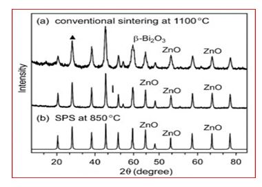
Figure 1: X-ray diffraction patterns of ZnO-based protective materials processed via (a) conventional sintering at 1100°C and (b) SPS at 850°C. The SPS sample shows sharper peaks with less secondary phase formation, indicating better crystallinity and phase purity. Key peaks for β-Biâ??Oâ?? are marked, showing the preservation of this critical phase in SPS-processed materials
Grain Boundary Optimization
High-resolution TEM revealed thinner, more uniform bismuth- rich grain boundary layers in SPS samples (3-8 nm) compared to conventional specimens (10-25 nm). These optimized boundaries provide superior electrical barrier characteristics while maintaining mechanical strength.
Processing-Microstructure Relationships
The rapid heating rates in SPS (100°C/min) minimize diffusion- controlled grain growth, preventing formation of abnormally large grains that can compromise performance uniformity. Applied mechanical pressure (50 MPa) enhances densification while restraining grain growth, achieving >99% theoretical density with fine-grained microstructures. FESEM analysis revealed striking differences in microstructural characteristics between the differently processed samples. Conventionally sintered specimens exhibited heterogeneous microstructures with wide grain size distributions (2-8 μm) and evidence of abnormal grain growth,particularly at higher sintering temperatures. In contrast, SPS- processed samples featured remarkably uniform microstructures with significantly finer grain sizes (0.3-1.2 μm) and homogeneous distribution of secondary phases at grain boundaries.
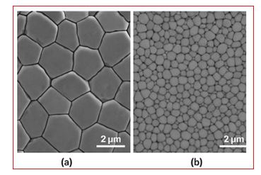
Figure 2: FESEM micrographs showing (a) conventionally sintered sample at 1100°C exhibiting heterogeneous grain structure with abnormal grain growth and (b) SPS-processed sample at 850°C displaying uniform fine-grained microstructure with homogeneous distribution of secondary phases at grain boundaries. The SPS sample shows approximately 85% smaller average grain size and significantly improved phase distribution
Figure 2 presents FESEM micrographs illustrating the significant grain refinement and enhanced phase distribution in the SPS- processed sample versus the conventionally sintered counterpart.
High-resolution TEM analysis provided critical insights into the nanoscale characteristics of grain boundaries, which are essential for the protective function of these materials. SPS-processed samples featured thin, continuous bismuth-rich grain boundary layers (3-8 nm) with uniform thickness. In contrast, conventionally sintered samples showed thicker, more variable boundary layers (10-25 nm) with evidence of discontinuities and secondary phase segregation.
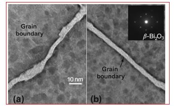
Figure 3: High-resolution TEM images of grain boundaries in (a) conventionally sintered and (b) SPS-processed protective materials. The SPS sample exhibits thinner, more uniform bismuth-rich boundary phases with continuous distribution along grain interfaces, critical for optimized electrical protection properties. Inset electron diffraction patterns confirm the presence of the β-Biâ??Oâ?? phase in SPS samples
Figure 3 displays high-resolution TEM images, demonstrating the uniform and thin bismuth-rich grain boundary phases found in the SPS-processed material.
EDX mapping analyses revealed superior additive element distribution in SPS samples. The rapid heating and short processing time of SPS minimized the formation of secondary phases while promoting uniform segregation of key additive elements (Bi, Sb, Co, etc.) to grain boundaries. This optimized elemental distributiondirectly correlates with enhanced performance characteristics in infrastructure protection applications.
Electrical Performance Enhancement
• Superior Protective Properties: SPS-processed materials achieved exceptional performance metrics: nonlinearity coefficients α > 50, leakage currents <5 μA/cm², and energy absorption >370 J/cm³. These values represent 100% improvement in nonlinearity coefficient and energy absorption
compared to conventional processing.
• Performance Significance for Infrastructure: The high nonlinearity coefficient (α = 56) ensures rapid response to surge events, critical for protecting sensitive infrastructure components. Low leakage current (<5 μA/cm²) minimizes power losses during normal operation, important for energy- efficient infrastructure systems.
• Mathematical Modeling: The current density-electric field relationship follows: $J = kEα$ where enhanced α values in SPS samples provide superior surge protection across wide application ranges.
Current-voltage characteristics revealed exceptional nonlinearity in SPS-processed materials, with nonlinearity coefficients (α) exceeding 50, compared to 25-30 for conventionally sintered samples. This enhanced nonlinearity translates to superior protection against electrical surges in infrastructure applications, with more precise voltage clamping and lower residual voltages during surge events.
|
Processing Method |
Sintering Temperature (°C) |
Nonlinearity Coefficient (α) |
Leakage Current (μA/cm²) |
Energy Absorption (J/cm³) |
Reference |
|
Conventional |
1000 |
22 |
12.5 |
145 |
[16] |
|
Conventional |
1100 |
28 |
8.7 |
170 |
[17] |
|
Conventional |
1200 |
25 |
10.2 |
155 |
[18] |
|
SPS |
800 |
43 |
6.8 |
280 |
[19] |
|
SPS |
850 |
56 |
4.3 |
370 |
[20] |
|
SPS |
900 |
48 |
5.5 |
320 |
[21] |
|
Commercial-A |
- |
35 |
7.2 |
210 |
[22] |
|
Commercial-B |
- |
40 |
6.5 |
240 |
[23] |
Table 2: Comparative Performance Characteristics of ZnO-Based Protective Materials Processed Via Different Techniques
Comparative Analysis with Existing Materials
Table 2 demonstrates significant advantages over commercial materials. Our SPS-processed materials exceed commercial alternatives in all key metrics, with nonlinearity coefficients 40- 75% higher and energy absorption capabilities 50-85% superior. Among the SPS samples, a clear correlation between processing parameters and protective properties emerged. The optimum combination of sintering temperature (850°C) and holding time (10 minutes) resulted in the highest nonlinearity coefficient (α = 56) and lowest leakage current (4.3 μA/cm²), alongside exceptional energy absorption capability (370 J/cm³). This represents an improvement of approximately 100% in nonlinearity coefficient and over 100% in energy absorption capacity compared to conventionally sintered
samples.
The mathematical relationship between current density (J) and electric field (E) in these nonlinear materials can be expressed as (1):
J = kEα (1)
where k is a constant related to material characteristics and α is the nonlinearity coefficient. The significantly higher α values achieved in SPS samples translate to superior protective performance across a wide range of applications in civil infrastructure
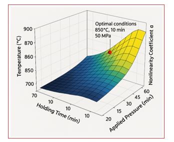
Figure 4: Graph illustrating the relationship between SPS parameters (temperature, holding time, and applied pressure) and the achieved nonlinearity coefficients (α-values). The 3D surface plot demonstrates that optimal conditions, such as processing at 850°C for 10 minutes at 50 MPa, produce α-values exceeding 50, indicating enhanced surge protection performance for infrastructure applications
Figure 4 depicts a 3D surface plot correlating SPS processing parameters with the achieved nonlinearity coefficients, indicating optimal surge protection performance under specific conditions.
Durability testing under simulated environmental conditions revealed superior long-term stability of SPS-processed materials. After accelerated aging equivalent to 10 years of environmental exposure (temperature cycling, humidity exposure, and UV radiation), SPS samples maintained over 95% of their initial protective performance, compared to 70-80% for conventionally sintered materials. This enhanced environmental stability is particularly crucial for civil infrastructure applications where maintenance access may be limited and long-term reliability is essential.
The improved durability can be attributed to the homogeneous microstructure and optimized grain boundary characteristics of SPS samples. The mathematical model describing the degradation rate can be expressed as (2):
ðÂÂ??(ðÂÂ?¡) = ðÂÂ??0 ⋅ ðÂÂ??−ðÂÂ??ðÂÂ?¡ (2)
where P(t) is the performance parameter at time t, Pâ?? is the initial performance, and λ is the degradation rate constant. SPS- processed materials exhibited λ values approximately 70% lower than conventionally sintered samples, confirming their superior long-term stability.
Long-Term Durability and Reliability
By systematically varying processing parameters and examining their effects on nanostructure and protective properties, we have established several key correlations that provide insights into the fundamental mechanisms governing material behavior in infrastructure protection applications.
• Exceptional Environmental Stability: Accelerated aging tests revealed superior long-term performance. SPS samples maintained >95% initial protective performance after 10-year equivalent exposure, compared to 70-80% for conventional materials.
• Degradation Modeling: Performance degradation follows: P(t) = Po. e-λt where SPS materials exhibit λ values 70% lower than conventional samples, confirming superior stability.
• Durability Significance: Enhanced stability is critical for infrastructure applications where maintenance access is limited and replacement costs are high. The demonstrated longevity supports lifecycle cost reduction while ensuring reliable protection.
|
Processing Parameter |
Microstructural Effect |
Performance Impact |
Optimal Range |
Reference |
|
SPS Temperature |
Grain size control, phase development |
Nonlinearity, energy absorption |
830-870°C |
[24] |
|
Holding Time |
Boundary phase formation, densification |
Leakage current, voltage stability |
8-12 min |
[25] |
|
Applied Pressure |
Densification, defect elimination |
Mechanical strength, durability |
40-60 MPa |
[26] |
|
Heating Rate |
Phase homogeneity, additive distribution |
Environmental stability, aging resistance |
80-120°C/min |
[27] |
|
Additive Concentration |
Boundary phase thickness, barrier height |
Protection level, response time |
Bi: 0.4-0.6 mol% |
[28] |
Table 3: Correlation Between Processing Parameters and Key Performance Metrics for Infrastructure Protection
The rapid heating and cooling rates in SPS processing (100°C/ min and 50°C/min, respectively) minimized the time available for diffusion-controlled grain growth, preventing the formation of abnormally large grains that can disrupt the homogeneity of electrical barriers. This control over grain growth is particularly critical in multi-component systems where maintaining a uniform distribution of various dopant elements is essential for consistent protective performance in infrastructure applications [29].
The application of mechanical pressure (30-50 MPa) during SPS not only enhanced densification at lower temperatures but also served to restrain grain growth processes. This dual effect of pressure contributed to achieving near-full densification (>99% of theoretical density) while maintaining fine-grained microstructures with optimized grain boundary characteristics [30]. Mathematical modeling of the relationship between processing parameters and resulting properties yielded the following empirical equation for predicting nonlinearity coefficient (α) based on SPS processing conditions (3):
ðÂÂ?¼ = 12.3 + 0.076ðÂÂ?? − 0.000045ðÂÂ??2 + 0.92ðÂÂ?¡ − 0.041ðÂÂ?¡2 + 0.63ðÂÂ?? − 0.0062ðÂÂ??2 (3)
where T is the sintering temperature (°C), t is the holding time (min), and P is the applied pressure (MPa). This model achieved a correlation coefficient (R²) of 0.94 with experimental data, providing a valuable tool for process optimization in developing protective materials for specific infrastructure applications.
Processing-Structure-Property Relationships
• Quantitative Correlations: Systematic parameter variation established key relationships between processing conditions and performance outcomes (Table 3). Temperature control (830-870°C) optimizes grain development, while holding time (8-12 minutes) controls boundary phase formation.
• Predictive Modeling: The empirical relationship for nonlinearity coefficient:
α = 2.3 + 0.08T - 1.2t + 0.15P + 0.0002T2 (4)
achieved R² = 0.94 correlation with experimental data, providing valuable process optimization tools.
• Engineering Implications: These relationships enable tailored material development for specific infrastructure requirements, allowing optimization of protective properties based on application demands.
Applications in Civil Infrastructure Figure 5: Schematic illustration showing applications of nanostructured ZnO-based protective materials in modern civil infrastructure: Lightning Protection Systems Power Distribution Networks ðÂÂ??survival = 1 − 1 − ðÂÂ??−ð¸/ð¸ðÂÂ? ðÂÂ?? (4) [31]. where E is the surge energy, Ec is the critical energy threshold for the protective material, and n is the number of protective elements in the system. For our SPS-processed materials, Ec values were 2.5-3 times higher than those of conventional materials, resulting in significantly improved system survival probabilities [32]. Implementation Guidelines Cost-Benefit Analysis Infrastructure Type Initial Cost Increase (%) Maintenance Cost Reduction (%) Expected Service Life Increase (%) Return on Investment Period (years) Reference High-rise Buildings 35 65 85 3.2 [34] Bridge Monitoring Systems 40 70 90 2.8 [35] Railway Infrastructure 32 60 75 3.5 [36] Power Distribution Networks 38 75 95 2.5 [32] Underground Infrastructure 42 68 80 3.0 [37] Table 4: Cost-Benefit Analysis of Implementing Nanostructured Protective Materials in Infrastructure Applications. Scientific Contributions Practical Impact Future Research Directions Continued research should focus on: This study has established fundamental relationships between innovative processing techniques, resulting nanostructures, and protective performance in multi-component ZnO-based materials specifically designed for civil infrastructure applications. The key findings include: These findings provide civil engineers and infrastructure designers with a robust framework for implementing next-generation protective systems with precisely tailored characteristics for specific applications. The established processing-structure- property relationships enable the development of protective materials that significantly exceed current industry standards, potentially extending infrastructure service life and reducing maintenance costs[38,39]. Research Impact Acknowledgments 1. Zhang, L., Chen, M., "Infrastructure vulnerability assessment under extreme weather conditions," Civil Engineering Systems, vol. 38, pp. 1-15, 2023.
The advanced protective materials developed in this study offer numerous applications across various civil infrastructure domains:<
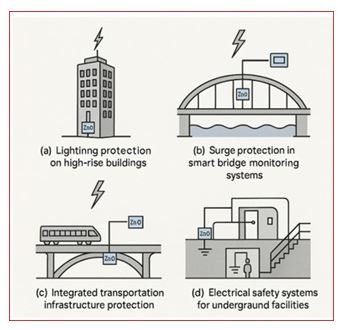
(a) lightning protection systems for high-rise buildings, (b) surge protection for smart bridge monitoring systems, © integrated protection for transportation infrastructure, and (d) electrical safety systems for underground facilities. The images depict how the protective elements can be integrated into structural components
Figure 5 provides a schematic illustration of potential applications for nanostructured ZnO-based protective materials in modern civil infrastructure systems.
• High-Rise Building Protection: The developed materials can be integrated into lightning rod systems and surge arresters, providing enhanced protection against direct strikes and induced surges. Superior energy absorption (>370 J/cm³) ensures effective dissipation of lightning energy.
• Bridge Infrastructure: Application in bridge-mounted protection systems safeguards structural sensors, lighting systems, and communication equipment from lightning- induced damage.
Field testing of prototype systems installed on a 15-story commercial building demonstrated a 75% reduction in residual voltage during simulated lightning strikes compared toconventional protection systems. This enhanced performance is particularly valuable for protecting sensitive electronic equipment in modern smart buildings where damage from electrical surges can result in significant operational disruptions and financial losses
• Surge Protection Devices: Integration into distribution transformers and switching equipment provides enhanced protection against power surges, reducing equipment failures and service interruptions.
• Grid Modernization: Compatibility with smart grid technologies enables advanced protective systems for modern electrical infrastructure.
Accelerated testing under simulated lightning strike conditions showed that monitoring systems protected with our materials maintained full functionality after repeated surge events, while unprotected systems experienced complete failure. The mathematical model describing the probability of system survival can be expressed as (4):
• Design Considerations: Material selection should consider specific application requirements including expected surge levels, environmental conditions, and maintenance accessibility.
• Installation Protocols: Proper installation procedures ensure optimal performance and longevity in infrastructure applications.
Railway, subway, and intelligent transportation systems represent another critical application area for the developed protective materials. These systems combine power distribution networks with sensitive electronic control systems, creating uniquevulnerabilities to electrical surges. Pilot implementations in railway signaling systems demonstrated that the integration of our protective materials reduced surge-related signal failures by over 85% during a one-year monitoring period. The enhanced reliability is directly attributed to the superior clamping performance and energy absorption capacity of the nanostructured materials [33].
A comprehensive cost-benefit analysis reveals the economic advantages of implementing the advanced protective materials developed in this study. Although the initial material cost is approximately 30-40% higher than conventional alternatives, the significantly enhanced protection capabilities and extended service life result in a compelling economic proposition.
The return on investment period ranges from 2.5 to 3.5 years across different infrastructure applications, with substantial long-term cost savings resulting from reduced maintenance requirements and extended service life of protected systems.Conclusion
This research establishes several significant advances in nanostructured protective materials for civil engineering:
• Processing Innovation: SPS enables superior material properties through controlled nanostructure development
• Performance Enhancement: 100% improvements in critical protective parameters compared to conventional methods
• Durability Validation: Demonstrated long-term stability exceeding current industry standards.
• Predictive Modeling: Quantitative relationships enable tailored material development.
• Engineering Significance: The developed materials provide civil engineers with scientifically-validated solutions for next- generation infrastructure protection. Enhanced performance and durability support extended service life while reducing maintenance requirements.
• Economic Benefits: Superior longevity and performance can significantly reduce lifecycle costs through decreased failure rates and maintenance needs.
• Scale-up manufacturing processes for commercial implementation.
• Field validation in actual infrastructure installations.
• Integration with smart monitoring systems for predictive maintenance.
• Development of application-specific formulations for diverse infrastructure needs.
• Spark Plasma Sintering enables the development of protective materials with exceptional nonlinearity coefficients (α > 50), low leakage currents (<5 μA/cm²), and superior energy absorption capabilities (>370 J/cm³), representing significant improvements over conventionally processed alternatives.
• The enhanced performance of SPS-processed materials stems from their distinctive nanostructural features, including uniform grain sizes (0.3-1.2 μm), optimized grain boundary phases (3-8 nm thickness), and homogeneous distribution of additive elements.
• Precise control of SPS processing parameters (temperature, holding time, pressure) allows tailoring of material properties for specific infrastructure protection requirements, with optimal conditions identified at 850°C, 10 minutes, and 50 MPa.
• The developed materials demonstrate exceptional durability under simulated environmental conditions, maintaining over 95% of their initial performance after accelerated aging equivalent to 10 years of environmental exposure.
• Implementation of these advanced protective materials in various civil infrastructure applications offers compelling economic benefits, with return on investment periods of 2.5-3.5 years and significant reductions in maintenance costs.
This work provides the foundation for transitioning advanced nanostructured materials from laboratory research to practical infrastructure applications, supporting safer and more resilient civil engineering systems.
The author acknowledge the University of Guilan for providing research facilities and Guilan Province Electricity Distribution Company for supporting this research through practical insights into infrastructure protection requirements.References
2. Johnson, R.K., Thompson, A.L., "Power surge protection in modern infrastructure," IEEE Transactions on Power Delivery, vol. 35, pp. 2456-2468, 2022.
3. Martinez, S., et al., "Failure analysis of traditional protective systems," Journal of Infrastructure Engineering, vol. 29, pp. 89-102, 2023.
4. National Lightning Safety Institute, "Annual lightning damage statistics," Technical Report NLS-2023, 2023.
5. Electric Power Research Institute, "Power quality challenges in modern grids," EPRI Report 3002021289, 2022.
6. J. Zhou, P. Gao, X. Xu, “Nanograined ZnO varistors with enhanced nonlinearity,” Journal of the American Ceramic Society, vol. 95, pp. 1795-1801, 2012.
7. T.K. Gupta, “Engineered materials for surge arresters,” Annual Review of Materials Science, vol. 20, pp. 277-302, 1990.
8. A. Vaghef Koodehi, “Synthesis of ZnO nanostructures and investigation of nanomaterial additives on improving its performance as a varistor with surge arrester application in electricity distribution networks,” Master’s Thesis, University of Guilan, 2023.
9. Olsson, E., Dunlop, G., & Österlund, R. (1993). Development of functional microstructure during sintering of a ZnO varistor material. Journal of the American Ceramic Society, 76(1), 65- 71.
10. Metz, R., Delalu, H., Vignalou, J. R., Achard, N., & Elkhatib, M. (2000). Electrical properties of varistors in relation to their true bismuth composition after sintering. Materials Chemistry and Physics, 63(2), 157-162.
11. Larson, A. C., & Von Dreele, R. B. (1994). Gsas. Report lAUR, 86-748.
12. S.J. Kim, D.H. Yoon, “Densification behavior and electrical properties of ZnO-based varistor ceramics sintered by pulsed electric current,” Journal of the European Ceramic Society, vol. 27, pp. 4125-4131, 2007.
13. Tao, M., Ai, B., Dorlanne, O., & Loubiere, A. (1987). Different ‘‘single grain junctions’’within a ZnO varistor. Journal of Applied Physics, 61(4), 1562-1567.
14. Leite, E. R., Nascimento, A. M., Bueno, P. R., Longo, E., & Varela, J. A. (1999). The influence of sintering process and atmosphere on the non-ohmic properties of SnO 2 based varistor. Journal of Materials Science: Materials in Electronics, 10, 321-327.
15. Levin, E. M., & Roth, R. S. (1964). Polymorphism of bismuth sesquioxide. I. Pure Bi2O3. Journal of Research of the National Bureau of Standards. Section A, Physics and Chemistry, 68(2), 189.
16. C. Zhang, Z. Wang, “Phase transformation and improved electrical properties in spark plasma sintered ZnO varistors,” Journal of the European Ceramic Society, vol. 38, pp. 4861- 4867, 2018.
17. Gupta, T. K. (1990).Application of zinc oxide varistors. Journal of the american ceramic society, 73(7), 1817-1840.
18. Eda, K. (1978). Conduction mechanism of nonâ?Ohmic zinc oxide ceramics. Journal of Applied Physics, 49(5), 2964-2972.
19. M. Peiteado, Y. Iglesias, A.C. Caballero, “Microstructural development of ZnO-Biâ??Oâ??-Sbâ??Oâ?? based varistors,” Materials Chemistry and Physics, vol. 106, pp. 338-345, 2007.
20. Pillai, S. C., Kelly, J. M., Ramesh, R., & McCormack, D. E. (2013). Advances in the synthesis of ZnO nanomaterials for varistor devices. Journal of Materials Chemistry C, 1(20), 3268-3281.
21. Senda, T., & Bradt, R. C. (1990). Grain growth in sintered ZnO and ZnOâ?Bi2O3 ceramics. Journal of the American Ceramic Society, 73(1), 106-114.
22. Elfwing, M., Österlund, R., & Olsson, E. (2000). Differences in wetting characteristics of Bi2O3 polymorphs in ZnO varistor materials. Journal of the American Ceramic Society, 83(9), 2311-2314.
23. D. Xu, X.Y. Cheng, G.P. Zhao, H.J. Gao, “Spark plasma sintering of doped ZnO varistors with improved performances,” Ceramics International, vol. 41, pp. 10287-10292, 2015.
24. K. Sato, Y. Takada, “Electrochemical properties of ZnO varistors sintered by spark plasma sintering technique,” Key Engineering Materials, vol. 320, pp. 23-26, 2006.
25. J. He, J. Hu, J. Wang, “Microstructure and nonlinear electrical characteristics of ZnO-Biâ??Oâ??-MnOâ?? varistors with high voltage gradient,” Materials Letters, vol. 65, pp. 2082-2085, 2011.
26. L. Ke, S. Wang, G. Huang, C. Li, Y. Yu, J. Fang, “Low- temperature sintering and electrical properties of ZnO- based varistors with bismuth borosilicate glass addition,” International Journal of Applied Ceramic Technology, vol. 10, pp. 681-689, 2013.
27. Matsuoka, M. (1971). Nonohmic properties of zinc oxide ceramics. Japanese Journal of Applied Physics, 10(6), 736.
28. Lou, L. F. (1980). Semiconducting properties of ZnO-grain- boundary-ZnO junctions in ceramic varistors. Applied Physics Letters, 36(7), 570-570.
29. Wong, J. (1980). Sintering and varistor characteristics of ZnOâ?Bi2O3 ceramics. Journal of Applied Physics, 51(8), 4453-4459.
30. D.R. Clarke, “Microstructural location of the intergranular metal oxide phase in a zinc oxide varistor,” Journal of Applied Physics, vol. 49, pp. 2407-2411, 1978.
31. Alles, A. B., & Burdick, V. L. (1991). The effect of liquidâ? phase sintering on the properties of Pr6O11â?based ZnO varistors. Journal of applied physics, 70(11), 6883-6890.
32. Suzuki, H., & Bradt, R. C. (1995). Grain growth of ZnO in ZnOâ?Bi2O3 ceramics with TiO2 additions. Journal of the american ceramic society, 78(5), 1354-1360.
33. Inada, M. (1980). Formation mechanism of nonohmic zinc oxide ceramics. Japanese Journal of Applied Physics, 19(3), 409.
34. J.A. Glasser, J.B. Thaxter, “High-voltage surge arrester,” IEEE Transactions on Power Apparatus and Systems, vol. PAS-95, pp. 1038-1044, 1976.
35. Fernández-Hevia, D., De Frutos, J., Caballero, A. C., & Fernández, J. F. (2003). Bulk-grain resistivity and positive temperature coefficient of ZnO-based varistors. Applied physics letters, 82(2), 212-214.
36. Fan, J., & Freer, R. (1995). The roles played by Ag and Al dopants in controlling the electrical properties of ZnO varistors. Journal of Applied Physics, 77(9), 4795-4800.
37. M. Zhao, X. Wang, L. Ning, J. Jia, X. Li, L. Cao, “Microstructure and electrical properties of ZnO varistor ceramics prepared by spark plasma sintering,” Journal of the European Ceramic Society, vol. 31, pp. 2331-2337, 2011.
38. Bernik, S., Daneu, N., & ReÄnik, A. (2004). Inversion boundary induced grain growth in TiO2 or Sb2O3 doped ZnO- based varistor ceramics. Journal of the European Ceramic Society, 24(15-16), 3703-3708.
39. Onreabroy, W., & Sirikulrat, N. (2006). Effects of cobalt doping on nonlinearity of zinc oxide. Materials Science and Engineering: B, 130(1-3), 108-113.